Introduction to IC Testing
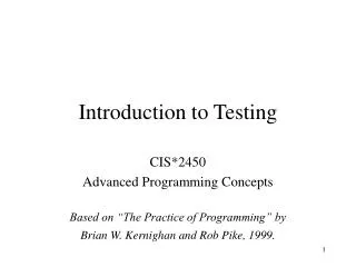
Introduction to IC Testing. Testing Goals : . Improve the reliability . Save money in manufacturing. Actual Device Input Circuit ( IIL , IIH). VDD. VDD. IIL leakage path. IIL. R ( ~ M ohm). P MOS. VSS VDD. VSS VDD. IIH. R ( ~ M ohm). N MOS. IIH leakage path. VSS= 0V.

Introduction to IC Testing
E N D
Presentation Transcript
Introduction to IC Testing Testing Goals : .Improve the reliability .Save money in manufacturing
Actual Device Input Circuit ( IIL , IIH) VDD VDD IIL leakage path IIL R ( ~ M ohm) P MOS VSS VDD VSS VDD IIH R ( ~ M ohm) N MOS IIH leakage path VSS= 0V
Actual Device Output Circuit ( VOL /IOL) VDD SPEC. IOL(MIN) =8.0MA VOL(MAX)= 0.4V R= E/I E=VOL-VSS R=0.4(V)/8(MA) R=50 OHM(MAX) VDD OFF OFF VOL Control ( 1 ) DUT Output Pin IOL E ON ON R IOL VSS= 0V
The device output pins must sink at least a specified amount of current and stay in the correct logic state SPEC. IOL(MIN) =8.0MA VOL(MAX)= 0.4V R= E/I E=VOL-VSS R=0.4(V)/8(MA) R=50 OHM(MAX) VDD VDD OFF OFF When IOL= 8MA Control ( 1 ) VOL 0.4 50 0.32 40 0.48 60 DUT Output Pin ON E ON R IOL VSS= 0V
Actual Device Output Circuit ( VOH /IOH) VDD(4.75V) VDD IOH IOH R ON E ON VOH Control ( 0 ) DUT Output Pin SPEC. IOH(MIN) =-5.2MA VOH(MAX)= 2.4V R= E/I E=VDD-VOH=4.75-2.4=2.35 R=2.35(V)/5.2(MA) R=452 OHM(MAX) OFF OFF VSS= 0V
Device Fanout Capability TTL Output Spec VOH=2.4V at-2.6mA VOL=0.4V at 24.0mA VOH =2.4V 2.6MA /150uA = 17.3 --> 17 VOL = 0.4 V 24 MA /0.8 MA= 30 TTL Output Spec IIL=0.8mA at 0.4V IIH=150A at 2.4V
Open Drain/Source Outputs OPEN DRAIN : output can only drive low - they only sink current OPEN SOURCE : output can only drive high - they only source current VDD VDD VDD External Resistor D D P MOS G Open Source Output G Open Drain Output S S External Resistor N MOS Open Source Open Drain Standard CMOS Cell
How to test a open drain device VOH (2v) IOL(~ 1uA) VDD VCM(4V) X External Resistor VOL(1v) D D G G Open Drain Output IOH S S Gate X 1 0v (L) 0 VCM(4V) (H)
How to test a open Source device VDD D G IOL S VDD VCM(0.5V) X D G Open Source Output VOH (2v) IOH(~ 1uA) S External Resistor Gate X 0 VDD (H) 1 VCM(0.5V)(L) VOL(1v)
L5710 Pin Electronics Block Diagram VIH PMU TO DUT DCL F_Ctrl VIL D_Ctrl VOH IOL Cmp_Hi L_Ctrl IOH VCM Cmp_Lo VOL
Truth table pattern A B 0 1 1 0 /* AB */ * 0H *; * 1L *; Connect to DPS VOH VIH VCC 7404 CMP_H 0/1 010101 HLHLHL A B CMP_L ON/OFF GND VIL VOL Connect to GND A TPDhl:Hi to Lo Propagation delay B TPDlh:Lo to Hi Propagation delay TPDhl TPDlh
VDD (a) set up time CLK (b) hold time DATA OUT DATA IN 100 ns 2.0 V (a) (b) CLK 0.8 V 2.0 V DATA IN Valid Data in 0.8 V 2.4 V DATA OUT 0.4 V
T0 0 T0 100ns T0 200ns T0 300ns T0 400ns 2.0 V DATA IN 0.8 V 2.0 V 0 1 0 1 DATA IN 0.8 V 2.0 V CLK 0.8 V H L 2.4 V L L DATA OUT 0.4 V Output strobe