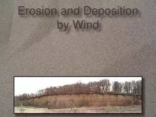
Download
1 / 26
370 likes | 828 Vues
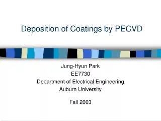
Deposition of Coatings by PECVD. Jung-Hyun Park EE7730 Department of Electrical Engineering Auburn University Fall 2003. Review of CVD. Film deposition by initiating a chemical reaction inside a chamber filled with reagents vaporized in an inert carrier gas

E N D
Deposition of Coatings by PECVD Jung-Hyun Park EE7730 Department of Electrical Engineering Auburn University Fall 2003
Review of CVD • Film deposition by initiating a chemical reaction inside a chamber filled with reagents vaporized in an inert carrier gas • Energy supplied by the surroundings causes the diffused reagents to react thus forming the desired material film across the target surface
Growing Steps of CVD • Gas phase Diffusion • Gas phase Reaction • Absorption • Surface Reaction • Surface Diffusion • Incorporation into the crystal lattice • Desorption • Gas phase Diffusion Reactant gases Exhaust gases (a) (h) (b) (g) (c) (f) (d) (e) Surfase http://www.postech.ac.kr/mse/tfxs/lecture_2000_1/chapter4.ppt http://cape.uwaterloo.ca/che100projects/vapourdep/sld001.htm
CVD Process Types • APCVD (simply CVD, atmospheric pressure CVD) :elevated temperature but at near atmospheric pressures (105 Pa) • LPCVD (low pressure CVD) :utilizes vacuum (< 10 Pa) to increase deposition rate and uniformity • PECVD (plasma enhanced CVD) :enhancing the reactions and permitting very low deposition temperatures
Question • What are the advantages/disadvantages of PECVD compared to other types of CVD process ?
APCVD Reactor • Advantages: • High throughput • Good uniformity • Handle large wafers • Disadvantages: • Fast gas flows • Needs frequent cleaning http://www.timedomaincvd.com/CVD_Fundamentals/Fundamentals_of_CVD.html
LPCVD Reactor • Advantages: • Excellent uniformity • Large load size • Hold large wafers • Disadvantages: • Low deposition rates • Toxic, corrosive or flammable gases http://www.timedomaincvd.com/CVD_Fundamentals/Fundamentals_of_CVD.html
PECVD Reactor • 50 kHz ∼ 13.56 MHz power source • Vacuum: 0.1~5 torr • Advantages: • Low deposition temperature • Low power source • Disadvantages: • Limited capacity • Individual wafer loading • Easily contaminated http://www.timedomaincvd.com/CVD_Fundamentals/Fundamentals_of_CVD.html
Why PECVD? (1) encourage deposition at much lower temperatures and pressures than would be required for thermal CVD. TEOS = tetraethyl orthosilicate, Si(OC2H5)4 http://www.batnet.com/enigmatics/semiconductor_processing/CVD_Fundamentals/plasmas/plasma_deposition.html
Why PECVD? (2) • The second reason to use plasma deposition is that surfaces exposed to a plasma are subject to bombardment by energetic ions, whose kinetic energy can vary from a few eV to 100's of electron volts. • Ion bombardment of this nature has very significant effects on the properties of the deposited film. Increasing ion bombardment tends to make films denser and cause the film stress to become more compressive • However, excessive compressive stress can also lead to impaired reliability. The ability to adjust stress, through changes in process conditions, chamber geometry, or excitation http://www.timedomaincvd.com/CVD_Fundamentals/plasmas/plasma_deposition.html
Why PECVD? (3) • A final important benefit of plasma deposition is the ability to easily clean the reactor. For example, by introducing a fluorine-containing gas (e.g. CF4) and igniting a plasma, one can clean silicon, silicon nitride, or silicon dioxide from the electrodes and chamber walls. • Chamber cleaning is of great practical importance; thick films built up on the parts of a chamber may create particles which can fall onto the substrates and cause defects in circuit patterns in semiconductor
Disadvantages of PECVD • Limited capacity : PECVD systems require wafers to lie flat on the bottom wafer. Only one wafer side can be coated at a time unlike LPCVD (wafers loaded vertically). PECVD can coat 1~4 wafers at one time whereas LPCVD can coat up to 25 wafers
Deposition of Organic Film • Plasma Polymerization • Amorphous Hydrogenated Silicon (a-Si:H) • Silicon Dioxide (SiO2) • Silicon Nitride (SiN) • Silicon Carbide (SiC) • Poly Silicon (poly-Si) • Diamond Like Carbon (DLC) Deposition of Inorganic Film Alfred Grill, Cold Plasma in Materials Fabrication, IEEE press
Plasma Polymerization • Atomic process • Polymers are most case highly branched and highly cross-linked • Strongly system-dependent process • Controlled under parameters – pressure, plasma, gas flow and applied electrical output http://www.eurobonding.org/Englisch/Oberflaechen/Plasma_polymerization.htm
Plasma Polymerization • characteristics - excellent coating adhesion on almost all substrates - chemical, mechanical and thermal stability - high chemical barrier effect • Applications - scratch resistant coatings - corrosion protection - anti-bonding, anti-soiling coatings - barrier layers http://www.vergason.com/pdfDocs/VTI%20papers,%20Plasma%20Polymerization,%20Theo.&%20Prac..pdf
Deposition of Inorganic Film • Diamond Like Carbon (DLC) capping material which exhibits radiation-hardening characteristics. devices developed for the military • Amorphous Silicon (A-Si) production of solar cells • Poly Silicon (poly-Si) Silicon Nitride (SiN) A-Si and poly-Si are conductive and depending upon their quantities having varying conductive properties http://www.plasmaequip.com/WHAT%20IS%20PECVD.pdf
Dielectric and Poly-Si Films • Most commonly used films • Poly-Si, SiO2, Si3N4 and SiNx • Most commonly deposition methods • APCVD, LPCVD, PECVD • Most common applications • Doped poly-Si as MOS gates • SiO2 as interlevel dielectric • Si3N4 as diffusion and sodium barrier • SiNx as chip passivation layer
Poly-Si Deposition • Reactor pressure can be controlled by • Pumping speed • Nitrogen flow • Total gas flow with constant ratio • Deposition reproducibility is best when the pressure is controlled by pumping speed http://www.engr.sjsu.edu/lhe/lectures/lecture%205(chap%2011-%20II).pdf
Poly-Si Deposition • Poly-Si films deposited below 580°C is amorphous • Poly-Si films deposited above 625°C is polycrystalline and has a columnar structure http://mmadou.eng.uci.edu/Classes/MSE621/MSE62101(14).pdf
SiO2 Step Coverage • TEOS at 700°C • Silane-O2 at 450°C and low P • Silane-O2 at 480°C and Atm. P file:///C:/Documents%20and%20Settings/joshua/Local%20Settings/Temporary%20Internet%20Files/Content.IE5/SX0PO7AF/445,7,Step Coverage over Trench
Properties of Deposited Nitrides • LPCVD nitride is stoichiometric and a good barrier against oxidation and sodium diffusion • PECVD nitride contains a large amount of hydrogen and can be etched with HF
Answer • Advantages: Lower substrate temperatures, Faster deposition rate, Good adhesion, Good step coverage, Low pinhole density • Disadvantages: Chemical and particulate contamination, limited capacity