Download
1 / 20
220 likes | 419 Vues
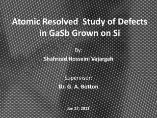
Atomic Resolved Study of Defects in GaSb Grown on Si. By: Shahrzad Hosseini Vajargah Supervisor: Dr. G. A. Botton Jan 27, 2012. Outline. Introduction Solar cell & Multijunctions Physical Properties & Crystal Structure Growth Techniques & Challenges

E N D
Atomic Resolved Study of Defects in GaSb Grown on Si By: Shahrzad Hosseini Vajargah Supervisor: Dr. G. A. Botton Jan 27, 2012
Outline • Introduction • Solar cell & Multijunctions • Physical Properties & Crystal Structure • Growth Techniques & Challenges • Importance of defects and their Identification Techniquces • Characterization Methods and Techniques • Results • Identification of Polarity Reversal and Antiphase Boundaries • Strain Analysis • Summary & Acknowledgment MATLS 702
Solar energy-power from the Sun Adopted from : http://eng3060.pbworks.com Increasing world consumption of energy Fossil fuel shortage Global warming Need for sustainable development Photovoltaic Effect Incident of Photons Generation of carriers by p-n junction movement of electrons to the n-type side and holes to the p-type side of junction Generation of voltage Efficiency: Ratio of number of carriers collected by solar cell to photons of given energy Adopted from : http://en.wikipedia.org/wiki
Physical properties & applications Sb-based Compound Semiconductors Adopted from : http://gorgia.no-ip.com/phd/html/thesis/phd_html/node4.html • Wide range of bandgap energies from 0.165 eV for InSb to 1.58 eV for AlSb • AlSb indirect and InSb and GaSb direct bandgap • High electron mobility and wide range of bandgap offsets Applications: • Multijunction solar cells • High speed electronic devices • Thermophotovolatic applications MATLS 702
Crystal structure Silicon (Substrate) GaSb (Film) Zinc-Blende structure Non- Centrosymmetric Wide range of bandgap energies Advantages: bandgap tunability • Diamond structure • Centrosymmetric • Advantages: low cost, large-scale integration and high quality MATLS 702
Thin film growth technique Molecular Beam Epitaxy (MBE) Features • Ultra high vacuum and controlled temperature condition • Effusion cells • Heated substrate • Different deposition ratio • In-situ surface analysis with Reflection High Energy Electron Diffraction (RHEED) Advantages • Abrupt interface • Highly precise controlling of doping levels Adopted from: http://department.fzu.cz MATLS 702
Growthchallenges • Lattice mismatch between film and substrate • Misfit dislocation • Relaxation of film • Planar Defects • Twins • Anti-Phase Boundaries (APB) • Polar on non-polar growth • Stoichiometric and non-Stoichiometric • Lowest formation energy {110}-type APB (Vanderbilt et al. 1992, Rubel et al. 2009) D. Cohen and C. B. Carter, Journal of Microscopy, 208(2), 84–99 (2002).
Why are defects so important? • Uncompleted or dangling bonds in the core of dislocations generate states near the middle of bandgap which are deep levels acting as recombination centers. • Elastic strain field of defects changes atomic distances and hence electronic states, acting as a trap. • Antiphase boundaries create non-radiative recombination centers. Reduction of efficiency of solar cell
APBs’ identification techniques with TEM -200 200 200-type Superlattice Reflections • Two beam Condition Dark Field Imaging Convergent Beam Electron Diffraction (CBED) Gowers, J. P. (1984). Applied Physics A Solids and Surfaces, 34(4), 231-236. S. Y. Woo(2012) et al. (Submitted) A. Beyer, I. Ne´meth, S. Liebich, J. Ohlmann, W. Stolz, and K. Volz, J. of Appl. Phys. 109, 083529 (2011) MATLS 702
APBs’ identification techniques with TEM High Resolution Transmission Electron Microscopy (HRTEM) images cannot be interpreted directly. Defocus Thickness Simulations show that the contrast highly depends on imaging condition Misidentification of APB with twin S. H. Huang, G. Balakrishnan, A. Khoshakhlagh, L. R. Dawson, and D. L. Huffaker, Appl. Phys. Lett. 93, 071102 (2008). MATLS 702 V. Narayanan, S. Mahajan , K.J. Bachmann, V. Woods, N. Dietz, Acta Materialia 50 1275–1287 (2002)
Research objectives To understand: • the atomic arrangements at antiphase boundaries • origin of the APB at interface • possible mechanism of APBs’ self-annihilation In order to: • prevent the APB formation, or • make them to self-annihilate MATLS 702
High Angle Annular Dark Field-STEM • Transmission Electron Microscopy Z-contrast (High angle annular dark field – HAADF) Scanning Transmission Electron Microscopy (STEM) • High angle elastically scattered electrons • Annular detector • Composition sensitive • Less sensitive to thickness and focus • Resolution is limited by lens aberrations: 1-Spherical (Cs) 2-Chromatic (Cc) • Advantages of using Aberration correctors: • Better Resolution • Reduced Contrast Delocalization • Sub-Å probe for spectroscopy • Tuning capability of Cs MATLS 702
Strained-layer superlattice (SLS) (a)Experimental HAADF-STEM Image (b) Multisclice Simulation of GaSb (c) Multisclice Simulation of AlSb GaSb AlSb MATLS 702
Polarity reversal Top views Side view MATLS 702
Edge-on APB twin GaSb APB Si Mixed Nucleation MATLS 702
Strain measurement technique Geometric Phase Analysis (GPA) In an image of perfect crystal intensity at each position like (r) can be written as Fourier sum which has amplitude and phase component. Degree of contrast of a set of fringe Lateral position fringes within image (Geometric phase) For a perfect crystal: Phase is constant across image For an imperfect crystal: Any lattice distortion or displacement causes local shift of fringes and consequently phase change or phase shift. Phase variations Local displacement field Strain Matrix MATLS 702
Strain distribution APB y twin x MATLS 702
Summary • Polarity reversal due to the formation of antiphase boundaries has identified directly for the first time with HAADF-STEM. • The direct identification of polarity reversal with HAADF-STEM avoids the misinterpretations in characterizing the planar defects. • The APB has formed due to the mixed nucleation at interface in spite of prior soaking with Sb. • Different bonding length in anti-phase bonds compared to in-phase bonds induces strain and lattice rotation at APB. • Compensating the lattice rotation by lateral shift and faceting can play an important role in the self-annihilation of the APBs. • Simultaneous control of the substrate misorientation angle and prelayer soaking step in growth can help to suppress the APB formation. MATLS 702
Acknowledgment • My supervisor: Prof. G. A. Botton • Research Group Fellows for helpful suggestions • Canadian Centre for Electron Microscopy (CCEM) staff • Ontario Center of Excellence (OCE) • Center of Emerging Device Technology for providing me with samples • Arise Technology for funding this project
Thank you ! Questions?