Download
1 / 13
1.02k likes | 2.16k Vues
Resonant Converters Introduction (1). Very large research area in Power Electronics Many ideas still in academia, but transfer to industry is being made Basic motivation is to reduce the switching loss in converters and to allow higher switching frequencies to be obtained

E N D
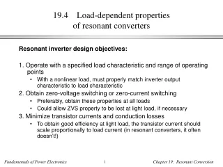
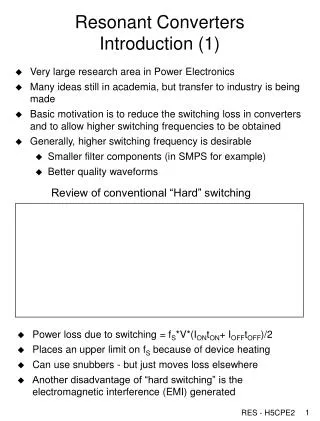
Resonant ConvertersIntroduction (1) • Very large research area in Power Electronics • Many ideas still in academia, but transfer to industry is being made • Basic motivation is to reduce the switching loss in converters and to allow higher switching frequencies to be obtained • Generally, higher switching frequency is desirable • Smaller filter components (in SMPS for example) • Better quality waveforms Review of conventional “Hard” switching • Power loss due to switching = fS*V*(IONtON+IOFFtOFF)/2 • Places an upper limit on fS because of device heating • Can use snubbers - but just moves loss elsewhere • Another disadvantage of “hard switching” is the electromagnetic interference (EMI) generated
Resonant ConvertersIntroduction (2) • Resonant converter techniques attempt to eliminate switching loss by using the properties of resonant circuits to arrange for V or I (or both) to be zero at the instant of switching • Very high operating frequencies have been reported - eg small power supply operating at 15MHz! • Hundreds of different topologies have been proposed which fall into 3 broad categories • Load Resonant - load forms part of a resonant circuit (see Mohan for examples) • Resonant Link Converters - not discussed further here (see Mohan for examples) • Resonant Switch Converters - Modifications of conventional circuits with a resonant circuit associated with each switch to give Zero Voltage (ZVS) or Zero Current (ZCS) switching • Load resonant and resonant switch circuits are the most often exploited • We will consider one resonant switch circuit in more detail - DC to DC forward converter with zero voltage switching
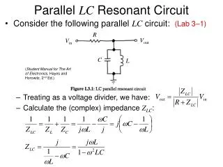
A Q Lf VO Cf D LOAD B Basic Forward Converter Circuit ZVS Forward Converter- circuit development A Q Lf L D2 VO Cf D C LOAD B Basic ZVS Forward Converter Circuit
A Q Lf L Io iL i D2 VO Cf D C LOAD VC B Basic ZVS Forward Converter Circuit A Q L i D2 IO E VAB D C VC B Circuit for analysis ZVS Forward Converter- assumptions for analysis • Assume ideal devices • Assume iL smooth so that iL= IO • VO = mean value of VAB
A L i IO E VAB C VC B Equivalent Circuit for Mode 1 ZVS Forward ConverterMode 1 • Before Mode 1 starts Q has been on for some time (see Mode 5) • Mode 1 starts when Q is turned OFF • Conditions at start of Mode 1: VC = 0, i = IO • IO charges C linearly VC rises linearly • VAB = E – VC when VC reaches E, VAB tries to go negative and D turns ON this ends MODE 1 • Duration for Mode 1 is given by:
A L i IO E D VAB C VC B Equivalent Circuit for Mode 2 ZVS Forward ConverterMode 2 • Conditions at start of Mode 2: VC = E, i = IO, D is ON • L and C form a resonant circuit (see separate analysis sheet) • VAB = 0, VC follows an offset sine, i follows a cosine:
A L i IO E D VAB C VC B Equivalent Circuit for Mode 2 ZVS Forward ConverterMode 2 continued D2 • Mode 2 finishes when VC tries to go negative and D2 turns ON • Duration for Mode 2 (2) can be found from: • Value of i (=I’) at the end of Mode 2 is given by: • I’ is negative
A Q L i D2 IO E D VAB C VC B Equivalent Circuit for Mode 3 ZVS Forward ConverterMode 3 • Conditions at start of Mode 3: VC = 0, i = I’ (negative), D is ON, D2 is ON • Resonance stops since C is shorted by D2 • VAB = 0, VC = 0 • Voltage across L = E i increases linearly (towards 0) • Q has a drive (Gate) signal applied during Mode 3, but doesn’t conduct immediately since i is negative • Mode 3 finishes when i reaches 0 and Q takes over i from D2 • Duration for Mode 3 is given by:
A Q L i IO E D VAB C VC B Equivalent Circuit for Mode 4 ZVS Forward ConverterMode 4 • Mode 4 starts when Q takes over i from D2 as it passes through 0 • Conditions at start of Mode 4: VC = 0, i = 0, D is ON, Q is ON • No resonance since C is shorted by Q • VAB = 0, VC = 0 • Voltage across L = E i increases linearly (towards IO) • Mode 4 finishes when i reaches IO and all of the load current is now flowing through Q D turns OFF • Duration for Mode 4 is given by:
A Q L i IO E VAB C VC B Equivalent Circuit for Mode 5 ZVS Forward ConverterMode 5 • Mode 5 starts when D turns OFF since Q has all the load current • Conditions at start of Mode 5: VC = 0, i = IO, D is OFF, Q is ON, D2 is OFF • No resonance since C is shorted by Q • Circuit is in steady state: VAB = E, VC = 0, i = IO • Mode 5 finishes when Q is turned OFF by the control circuit back to Mode 1 • Duration for Mode 5 is controllable and provides the means for controlling the output voltage Vo (= mean value of VAB)
ZVS Forward Converter Observations • At the instant at which Q turns OFF, the voltage across it is held at virtually zero by C No turn-off loss (ZVS) • At the instant at which Q starts to conduct (end of Mode3), the voltage across it and the current through it are both zero No turn-on loss (ZVS and ZCS) • ZVS at turn-on is only possible if V E • V IO circuit must be designed for lowest IO • If the range of IO is large, V will be much larger than E at the maximum current • Q will see a very large voltage when it is off. This is a disadvantage of this particular circuit • Can be partially overcome at the expense of more complexity • To control VO, we can only control the time for Mode 5 (5) • 1 4 are set by the circuit parameters and the output current • Control is more complex than for normal (non ZVS) circuit since both the duty cycle and operating frequency must be varied • Output voltage is given by:
Resonant Converters General Observations • ADVANTAGES • Virtually zero switching loss • High operating frequencies possible • High efficiencies • Soft switching - reduced EMI • DISADVATAGES • More components • More complex control • Increased voltage and/or current stress on devices • Possibility of increased conduction loss (can partially outweigh reduction in switching loss)