
Clock Sync Distribution & Streaming Readout TDC Study | JLAB Trigger Clk Sync Overview
Explore clock recovery studies for clock jitter measurements and clock wandering issues in a streaming readout setup. Understand clock/Sync distribution and VETROC streaming TDC principles. Discuss clock cleanliness and synchronization efficiency.

Clock Sync Distribution & Streaming Readout TDC Study | JLAB Trigger Clk Sync Overview
E N D
Presentation Transcript
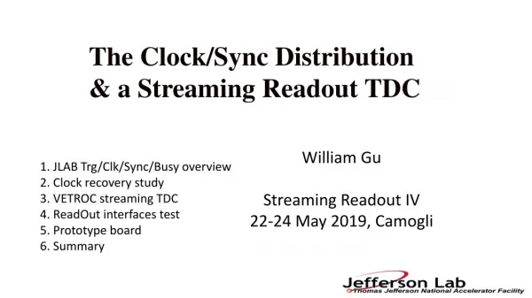
The Clock/Sync Distribution & a Streaming Readout TDC William Gu Streaming Readout IV 22-24 May 2019, Camogli 1. JLAB Trg/Clk/Sync/Busy overview 2. Clock recovery study 3. VETROC streaming TDC 4. ReadOutinterfaces test 5. Prototype board 6. Summary
1. JLAB HallB/D Trg/Clk/Sync/Busy overview TS SD MTP Fiber assignment: (TS) Trigger Supervisor TD (up to 16) Trigger etc. Signal Distribution VXS backplane Clock (TD) Trigger Distribution Sync FiberMeas TI (front end) TS/TD FiberMeas MTP fibers ~60 Not_used Not_used Acknowledge/Busy • Same clock forthe system; • Frontend electronics is Synced to one clock period (4 ns); • Delay adjustment on TI to compensate for the fiber delays; • Clock jitter: several ps (TI) Trigger Interface TI Signal Distribution VXS backplane FrontEnd TDC/ADC FronEnd Readout electronics
2. Clock Recovery Study 2.1 Low jitter clock can be recovered Mellanox 10 GBE Xilinx KCU040 312.5 MHz Mellanox (10 GBE) Fiber Xilinx KCU105 (UltraScaleKintex) Co-ax/copper Recovered clock to Tektronix DPO7254 Tektronix DPO7254 Clock result: Period: 3.2000ns, Frequency: 312.50 MHz Std Dev: 3.28 ps, 320.2 KHz P_P: 29.3ps, 2.86 MHz Enabling the Mellanox TX, Std Dev 3.30 ps Enabling the KCU040 TX, Std Dev 6.42 ps Single pulse period measurement: Std Dev: 6~7 ps DPX mode (200 GSps): 700~900 fs
2. Clock Recovery Study 2.2 OneTwo clock recovery Xilinx KCU1500 6.25 Gbps VETROC Xc7a200 312.5/2 QSFP transceivers/Fiber Xilinx Aurora-64B66B & Aurora-8b10b VETROC Xc7a200 312.5/2 Clock result: Period: 6.4000ns, Frequency: 156.25 MHz Std Dev: 10.02 ps, 244.6 KHz P_P: 85ps, 2.08 MHz Single pulse period meas.: Std Dev: 7.5 ps DPX mode (200 GSps): 778 fs *VETROC FPGA Scope: long LVCMS, then differential PCB traces. 312.5 MHz impossible
2. Clock Recovery Study 2.3 Clock wandering probem • Trigger on the VETROC_A recovered clock, the VETROC_B recovered clock width P_P is about 200ps ! • All these four channels are reconstructed KCU1500 clock • Ch#1 and Ch#2 have narrow spread as ch#2 is the trigger source • Ch#3 and Ch#4 have wide spread (~200ps) • Ch#2: Width: 6.4ns, Std Dev: 1.71ps • Ch#4: Width: 6.4ns, Std Dev: 2.54ps • The phase between Ch#1/2 and Ch#3/4 are changing (within a clock cycle) when re-link, though the phase is pretty stable. This is caused by the CDR clock devision. Ch#1: VETROC_A, MGT#2 RxClk, single-ended probe Ch#2: VETROC_A, MGT#3 RxClk, differential probe Ch#3: VETROC_B, MGT#2 RxClk, single-ended probe Ch#4: VETROC_B, MGT#3 RxClk, differential probe
2. Clock Recovery Study 2.3 Clock wandering probem (continued) • The difference between two reconstructed clocks. • The width of the difference of the two reconstructed clocks from the SAME vetroc board is measured to be (one differential probe): • Width: 336 ps • Std Dev: 3.75 ps • The width of the difference of the two reconstructed clocks from two VETROC boards is measured (two differential probes with scope math) to be: • Width: ~472/822 ps (mean 458/781 ps) • Std Dev: ~35/50 ps (p_p ~210/347 ps) • (Positive/Negative, not precise meas.)
2. Clock Recovery Study 2.3 Clock wandering probem (continued) Fundamental problem: TIE (Total Interval Error), not jitter. The TIEs are asynchronous among the recovered clocks. The recovered clock depends on the data protocol (consecutive number of 1s or 0s in the data stream) A typical clock recovery circuit • ADC measurement effects: • Clock Jitter affects the measurement precision; • The TIE effect is not critical • TDC measurement effects: • The TIE affects the measurement precision (channel to channel alignment, unless a precision common signal is used as the time reference); • The jitter effect is not critical as the jitter is much smaller than the TDC measurement precision • Data transmission effects: • Clock Jitter affects the data transmission; • The TIE effect is not critical
2. Clock Recovery Study 2.4 Clock/Sync distribution tree It is not expensive ($50 for a 40 Gbps optic transceiver) to keep QSFP (easy) for Clock/Sync distribution and streaming data readout Dedicated clock to keep the edge information (low jitter, no wandering), but, we will keep an eye on the LpGBT development at the LHC MTP Fiber assignment: Something? (10GBE TCP/IP etc.) Clock Sync Clock extraction, Clock cleanup, Sync etc. FiberMeas /Data/Backpressure Computer (Event ID) Detector (front end) FiberMeas / Streaming Data Streaming Data Streaming Data Streaming Data
3. VETROC Streaming TDC 3.1 TDC measurement principle Ch_In One CLB One CLB One CLB One CLB Carry Chain 33x4 units Calib_In • The edges of the pulse is measured against the system clock: • precision part: phase in the clock (using Xilinx FPGA carry chain delay and clock registers); • coarse part: number of clock cycles since system reset (T_zero) (a synchronous counter) Calib_sel Register 132 DoubleClock 500MHz FD FD FD FD FD FD FD FD FD FD FD FD FD FD FD FD FD FD FD FD Rising/Falling edge finder Pipelined edge position encoder Fine_Time(5:0) Rising edge Falling Edge Clock 250MHz Fine_Time(5:0) Falling edge Rising edge Detect the edge phase (relative to the 250 MHz clock) Edge Detected FineTDC(7:0) Valid Fine Time CoarseTime Free running timer, (one timer for all channels) “ZERO” suppressed SYNC (T_zero) TDC data/Data Valid
3. VETROC Streaming TDC Data Format (128 bits) Bits (127-124) (123:104) (103:78) (77:52) (51:26) (25:0) TYPE Timer Ch#ACh#BCh#CCh#D Timer(28:9) 3.2 VETROC Streaming TDC Ext_Calib_In ( 25:20 : 19:8 : 7 : 6 : 5 : 0 ) CH# Coarse_time Clk250 pulse Fine_time 0-63 Time(11:0) edge edge ~35ps Ref_Ch_In VME 64 32-channels LVDS inputs 32-channels LVTTL inputs • Bit(127:124) decoding: • 0x8 for channels 1-32; • 0x9 for channels 33-64; • 0xA for channels 65-96; • 0xB for channels 97-128; • 0xF for reference channels xc7A200 FPGA 4*6.25 Gbps Streaming outputs 32-channels LVDS inputs For reference channels, the full 48-bit timer is included, which keeps the unique time for about 290 hours after SYNC. 32-channels LVTTL inputs
3. VETROC Streaming TDC (backup slide) Edge separation: <2.5ns; LSB: ~35ps; TimeStamp: ~10 days; Streaming rate: ~2.5 Gbyte/s Channel count: 128 3.2 VETROC Streaming TDC – 128 TDC channels with extra reference channels Timer(11:0) Timer(28:9) Timer(47:0) Clock 250 MHz Ch#1 data(19:0) Clk 250 MHz /20 Computers do not recognize the AURORA data stream Merged data(127:0) 128(wide) x 1024(deep) Channels 1-4 Ch#2 data(19:0) /20 /20 Ch#3 data(19:0) /20 Merges the eight Streams to one (127:0) (round robin) And buffer in memory Two 41, empty control One 21, timer control Merged data(127:0) 128(wide) x 1024(deep) Channels 5-8 Ch#4 data(19:0) /128 128 Data merging and Clock domain transition. Aurora_8b10b 3x128 MGT (4*6.25Gbps) /20 Ch#32 data(19:0) Channels 29-32 128 QSFP fiber Ch#33-64, 65-96, 97-128 Ref_Ch
4. Streaming Readout: 4.1 10-GBE test using KCU105 eval board 10 GbEto a Mellanox card (UDP) and skip the 802.2 header: Reached: ~1.1 GByte/s(sustained) (from ifconfig ?trusted?)
4. Streaming Readout: 4.2 xDMA PCIe3x8 test using KCU1500 accelerator card Using Xilinx’s PCIe DMA driver, and modified test software: QSFPs: Aurora 8-lane, 8x10 Gbps, 64b66b encoding, loopback through fiber • Achieved on the computer: • Computer (memory) KCU1500: 5600 MB/s • ANDKCU1500 Computer (memory): 5200 MB/s.
4. Streaming Readout: ARISTA 7170-32C KCU1500 In ALKAID 4.3 TCP/IP readout (INDRA lab setup) KCU1500 ARISTA 7170-32 TCPIP 10 GBE Aurora 8b10b TCPIP 10 GBE 20 gb/s Graham’s Stream_Router ~400 Mbyte/s VETROC TDC MLX 10GBE MLX 10_GBE in INDRA-S2 VETROC TDC In VXS crate
4. Streaming Readout: computer 10 GBE 4.4 KCU1500 functional diagram Reg(31:0) Mon(127:0) Double PCIe3x8(xdma) 10 GBE IN QSFP RX TX D1(31:0) Duplicate Aurora 20 gbps 10 GBE IN FIFO StreamTDC QSFP (4x6.25gbps) D2(31:0) 10 GBE IN OUT D3(31:0) IN 10 GBE(TCP/IP) Playback ROM Merge Data_Sel QSFP TX RX DB(127:0) ARISTA 7170 MLX 10GBE/Computer * The Data flows are in parallel
5.Prototype board: 5.1 STDCpcie Two QSFPs (2x4x10 GbE Or 2x40 GbE Or others) PRELIMINARY 32 LVDS inputs + 10MHz clock Clock, Sync Combining the VETROC streaming readout TDC and the KCU105 into one: 64-CH Streaming TDC with standard interfaces (PCIexpress_Gen3 and Ethernet_10GBE) XCKU040-2 PCIe3x8 (64 Gb/s) 32 LVDS inputs + SYNC 12-layer, PCIe x8 or VME (~3U)
5. Prototyping board: 5.2 STDCpcie Status • This board will be able to test: • Standalone 64-channel streaming TDC (~20ps) with up to eight 10 GBE interfaces; • 64-channel TDC PCIe Gen3 x8 interface; • Sync/clock/Readout test of many boards (system) with the proposed fiber assignment (sec. 2.4); • 8x MGT (1 Gbps ~ 16 Gbps) PCIe3 x8; • 4x MGT (1 Gbps ~ 16 Gbps) 4x 10 GbE; • Serial link beyond 10 Gbps (PCIe GEN4, 25_GBE/100_GBE) with more advanced FPGAs; The board is ready to be manufactured: the PCB is fully routed and DRC checked; budget secured.
6. Summary: • The CLOCK/SYNC distribution is feasible • The dedicated clock distribution tree is better and easier, and cost manageable; • The SYNC can be accomplished with the fiber length measurement, and delay compensation; • We will keep an eye on the CLOCK/SYNC developments (LpGBTetc.); • The STREAMING READOUT is feasible • A 128-ch Streaming TDC is tested; • Some readout interfaces are tested; • Several (prototype) boards will be manufactured for CLOCK/SYNC/StreamingTDC test Thank You