Smart Dust: Unique Low Power Flexible Sensor Network
210 likes | 224 Vues
Smart Dust is a unique and low-power sensor network composed of tiny dust particles that communicate wirelessly and perform distributed computations. This article discusses the challenges and solutions in designing and implementing the Smart Dust network, including the design of physical dust particles, development of communication protocols, and data fusion techniques.

Smart Dust: Unique Low Power Flexible Sensor Network
E N D
Presentation Transcript
Smart Dust: Unique Low Power Flexible Sensor Network Neil Goldsman, Haralabos (Babis) Papadopoulos and Shuvra Bhattacharyya Dept. of Electrical and Computer Engineering University of Maryland College Park
Lead Personnel All UMD ECE Faculty Prof. Neil Goldsman Director of ECE Mixed Signal VLSI Lab Director of ECE Semiconductor Simulation Lab Introduced RF VLSI Circuit Design to UMD Other Areas: 3D Integration (with LPS) Prof. Haralabos (Babis) Papadopoulos Institute for Systems Research Communications and Signal Processing Laboratory Center for Satellite Communications Other Areas: Power Efficient Private Comm. Networks Prof. Shuvra Bhattacharyya Institute for Advanced Computer Studies Digital VLSI Design Automation Laboratory Embedded Systems Research Laboratory, Communications and Signal Processing Laboratory Other Areas: Embedded Software; Low Power Design
Outline • Smart Dust Overview • Electronics (Neil) • RF VLSI, Hardware, Sensors and 3D Integration • Communications (Babis) • Algorithms and Signal Processing • Microcontrol (Shuvra) • Digital Hardware and Software for Data Flow and Processing
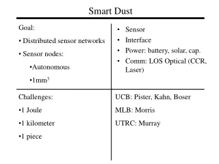
Overview: Smart Dust Network • A network of smart sensors (dust particles) that communicate with each other wirelessly and perform distributed computations. • Dust particle to be mm size (grain of sand). • Network to be seamlessly integrated into environment for flexible application. • Each dust particle usually contains a sensor, a micro-controller, a transceiver, and powering mechanisms • The network can contain several hundreds or even thousands of dust particles.
Overview: What is a Smart Dust Network? • The dust particles sense physical attributes of the environment, and then wirelessly communicate these attributes to other dust particles. • Using a distributed computing algorithms, the dust particles fuse their data, and make decisions based on the cumulative information of the overall network. • Applications: • Motion and Distance tracking • Biological and Chemical Environmental Factors • Distributed Image Recognition and Optical Sensing • Acoustic and Vibrational Sensing
Overview: The Challenges • Dust particles are small size but must still house RF and computational circuitry. • Low Power: Dust particles are either to be powered externally or by a power source that is commensurately sized with respect to the dust particle. We must perform RF communication, computations and sensing which minimize power use, but still overcome noise limitations and bit errors. • How to physically produce dust particles that allow for sensing, communication and computation on a system that is millimeter scale? • What special computational codes and hardware do we need, and what special communication algorithms do we need?
Overview: Overcoming the Challenges GOAL: To develop a state-of-the-art smart dust system Logistics: We have divided the project into three major tasks. • Design of Physical Smart Dust Particles: Circuits and Sensors (Neil). • Development of Network Communication Protocols and Fusion of Data (Babis). • Computation for Data Analysis and Network control (Shuvra).
Design of Physical Smart Dust Particle Particles:Circuits and SensorsNeil Goldsman
Tx Sensor ADC Rx L1 μP L2 Dust Particle Basic Topology Achieve with State of Art CMOS, Novel Materials (CNTs) & Unique 3D Integration. • Sensor: Optical, Biological, Temperature, etc. (analog) • μP: microprocessor (control and signal processing) • Tx, Rx: Transceiver
LNA PA BPF IMF IFF Use Phase-Locked Loop-Based Transceiver Rx DEMOD Series to Parallel 1,0 CPU Sample CLK f1-f2= f2-f3= f3-f1= …. PLL N,N+1,N+2,… N,N+1 Tx MOD & Carrier
PLL Reference Frequency Output Dual Modulus Prescaler Digital Input A/D Converter Shift Register Analog Input Clock Data Sampling Rate Background: FSK PLL VLSI Chip Already Developed
PLL Output MeasurementsLow Phase Noise, Nice Lock Frequency: 50MHz 500MHz 100MHz PhaseNoise: -1.6dBc/Hz -1.8dBc/Hz -2.2dBc/Hz 20.8dBc/Hz 16.5dBc/Hz -1.4dBc/Hz
Analog Structures for Meeting Low Power, Small Size Dust Design Constraints • Operating frequency high GHz for small dimensions • On-Chip antenna tuned to high GHz • Transceivers rely heavily on tuned circuits • Need State of Art Inductors for Max Q and Min Area. • 3D inductor and Antenna design • Carbon Nanotube Kinetic Inductor (2nd generation) • RF MEMS Resonator (2nd generation) • Sensors • On chip temperature sensor array • Optical diode array (visible and infrared) • MEMS accelerometer, microphone (2nd generation) • On-chip microwave power harvester • Antenna and Schottky diode form power supply Assemble into Single Dust Particle with Novel 3D Integration Methods
Achieving Smart Dust with 3D Integration • To integrate sensors, RF, and processors into a millimeter size system, 3D integration is a likely approach. • We can build on our existing research in this area with LPS (G. Metze). • Integration achieved through modular levels. 1mm Three-Dimensional Integrated Dust Particle
3D Inductor and Transformer Test Structures Prototype fabricated in 0.5μ CMOS with MOSIS. Simulations indicate 3D structures have much larger L and Q Currently being verified experimentally a with network analyzer.
Prototyping Temperature Sensor Array (10x10) Diodes are used as temperature sensors: Diode current increases exponentially with temperature. Fabricated in 0.5μ CMOS
3-D Prototyping Stacking Chip • New chip with structures that can connect in 3D. • Uses Symmetric Vias for 3D Interconnects” • Prototype fabricated in 0.5μ CMOS with MOSIS.
Proof of Principle Prototype • Develop Temperature Sensor Smart Dust Network • Use aforementioned RF and Temperature Systems • Employ State of the Art Dust with 3D Integration • Power • First with batteries • Second by harvesting the environment (RF, Heat) • Communication and Microcontrolling schemes to be used are described next.
Related Recent Publications • A. Akturk, N. Goldsman and G. Metze, ``Faster CMOS Inverter Switching Obtained withChannel Engineered Asymmetrical Halo Implanted MOSFETs, Solid State Electronics, vol. 47, pp.~185--192, 2003. • X. Shao, N. Goldsman, O. M. Ramahi, P. N. Guzdar, A New Method for Simulation of On-Chip Interconnects and Substrate Currents with 3D Alternating-Direction-Implicit (ADI) Maxwell Equation Solver. International Conference on Simulation of Semiconductor Processes and Devices, pp. 315-318, 2003. • 3. X. Shao, N. Goldsman, and O. M Ramahi, The Alternating-Direction Implicit Finite-Difference Time-Domain (ADI-FDTD) Method and its Application to Simulation of Scattering from Highly Conductive Material, IEEE International Antennas and Propagation Symposium and USNC/CNC/URSI North American Radio Science Meeting: URSI, Digest, p. 358, 2003. • Y. Bai, Z. Dilli, N. Goldsman and G. Metze, Frequency-Dependent Modeling of On-Chip Inductors on Lossy Substrate, International Semiconductor Device Research Symposium, pp. 292-293, 2003. • 6. X. Shao, N. Goldsman, O. M. Ramahi,and P. N. Guzdar, Modeling RF Effects in Integrated Circuits with a New 3D Alternating-Direction-Implicit Maxwell Equation Solver, International Semiconductor Device Research Symposium, pp. 532-533, 2003. • A. Akturk, L. Parker, N. Goldsman, G. Metze, Mixed Mode Simulation of Non-Isothermal Quantum Device Operation and Full-Chip Heating, International Semiconductor Device Research Symposium, pp. 508-509, 2003. • G. Pennington and N. Goldsman, Semiclassical transport and phonon scattering of electrons in semiconducting carbon nanotubes, Phys. Rev. B, 68 (4): Art. No. pp. 045426-1 -- 11, 2003.
Unique Aspects of Project 3 PI’s form Complementary & Unique Skill Set • 3D Integration for Dust • RF VLSI Design & Chip Electromagnetics • Semiconductor Physics and Novel Structures • Embedded μP Systems • Low power, memory-constrained implementation techniques • Application-specific optimization of software and VLSI • Integrated optimization of protocols and system configuration • Distributed Fusion Wireless Networks • Low power, scalable, fault tolerant, locally constructed. • Optimized source encoding algorthms