EE 392 I Field Programmable Technology for Mainstream Processing
EE 392 I Field Programmable Technology for Mainstream Processing. Gordon Brebner Xilinx Research Labs. What this talk is about. Overview of the Field Programmable Gate Array (FPGA) Processing opportunities for FPGAs The relationship between FPGAs and CPUs Programming models for FPGAs.

EE 392 I Field Programmable Technology for Mainstream Processing
E N D
Presentation Transcript
EE 392 IField Programmable Technology for Mainstream Processing Gordon Brebner Xilinx Research Labs
What this talk is about • Overview of the Field Programmable Gate Array (FPGA) • Processing opportunities for FPGAs • The relationship between FPGAs and CPUs • Programming models for FPGAs
Field programmable technology • “Field programmable” means “programmable in the field” • In other words, it is a “soft hardware” technology • Lingering historical stereotype: • More advanced stereotype: the sea of programmable logic gates • Today’s focus: the Field Programmable Gate Array (FPGA) The Programmable Logic Array (PLA)
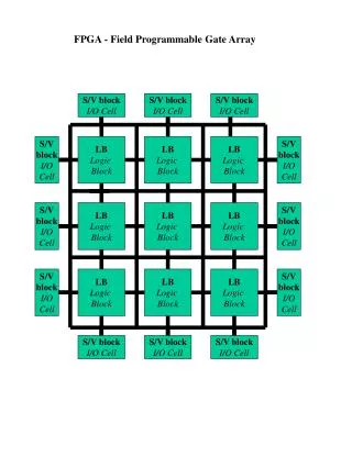
A contemporary FPGA: the Xilinx Virtex-6 • Example: XC6VHX565T • 566,784 programmable logic cells • 32.832 Mb block memory • 864 DSP blocks • 720 parallel input/outputs • 24 GTH transceivers (to 11.2G) • 48 GTX transceivers (to 6.6G) • 4 PCI Express blocks • 4 Tri-mode MAC blocks • Importantly, the components are interconnected by a very large amount of programmable wiring Programmable logic Block memory DSP block High performance clocking Parallel input/output High-speed transceiver PCI Expressinterface Tri-mode Ethernet MAC System Monitor
Original FPGA use situations • Prototyping ASICs • Classic style of chip design flow • Generate FPGA programming information instead of mask data • Providing glue logic for systems • Implement random logic to connect together other chips • Typically small-scale functions • Implementing input/output interfaces • Do heavy lifting for getting bits in and out quickly • Exploit the support for numerous physical i/o standards
Positioning FPGAs for mainstream processing • Moving the FPGA to the heart of the system • As a first-order processing component • Background: FPGAs have the raw processing capacity • Approaching millions of programmable logic cells • Other hardened processing components • Embedded memory blocks • Question: how do you organize this low-level capacity? • What soft processing architectures might be configured? • How can a high level programming experience be provided?
FPGAs for Digital Signal Processing (DSP) • Best known FPGA processing domain: streaming data flow • Low level: filters, DFT/FFT, coders/decoders, etc. • High level: wireless (e.g. 802.16, LTE), video (e.g., H.264, MPEG) • Example of benefit:
FPGAs for High Performance Computing (HPC) • Increasing area of application • Enabled by the increasing capabilities of FPGA • Scale down supercomputing techniques to FPGA-style parallelism • Example areas: • Finance: automated stock trading, etc. • Bioinformatics: gene sequencing, etc. • Cryptography • Meteorology • Lack of native support for floating point arithmetic has retarded adoption in certain areas SAN JOSE, Calif., April 6, 2010 Xilinx Helps University of Regensburg Launch the World's Most Power-Efficient Supercomputer … QPACE; a bespoke supercomputer developed to unlock the mysteries of Quantum Chromodynamics.
Network processing contexts NIC card Standalone switch/router Telecom line card
The NetFPGA platform netfpga.org • Stanford/Xilinx collaboration • Worldwide teaching and research ecosystem • Four gigabit Ethernet ports; PCI interface to host PC • Four x 10G version imminent
Processing on a telecom line card Police and shape flow rates Queue and schedule packets Frame data in physical blocks Compute error check codes PHY Framer / MAC / Mapper Packet Processor Traffic Manager Bridging / Backplane Interface Optics Backplane Classify packets into flows Parse and edit packets
FPGAs for Network Processing • Physical line interface and backplane interface • Standard input/output interfacing use case for FPGAs • Framing and error checking • Moving bits to the right places • Computing standard coding functions • Packet processing • Classification: computing hashing functions, lookup in binary/ternary CAM • Inspection and surgery: programmable parsing and editing of packets • Traffic management • Moving packets to the right places, and storing them • Computing policing and scheduling functions • Functions can be carried out at line rates of 100 Gb/s and above
Example of FPGA in virtual networking node High reliability sensor network High speed e-science network Highly secure network Virtual node 2 Virtual node 3 Virtual node 1 Triply redundant datapath High throughput data plane Security algorithm acceleration Dynamically managed physical Hardware
Relationship between FPGAs and CPUs • FPGA processing and CPU processing are complementary • FPGA better for bit-level, high-speed streaming, regular, settings • CPU better for word-level, random access, irregular, settings • Processors can be embedded into FPGAs • Hardened in the silicon • Example: PowerPC included in several Xilinx Virtex generations • Example: ARM – just announced by Xilinx today • Soft • Built out of programmable logic • Can now fit in multi-core architectures with 100s of processors • In principle, programmable logic can be embedded into CPUs
Cohabitation model #1: Instruction acceleration • CPU instruction set augmented by custom instructions • When a custom instruction is executed: • Instruction operands are presented over a CPU data bus • Become inputs to a processing block on the FPGA • Processing operation is carried out • Outputs directed from processing block to data bus • Instruction result(s) are obtained from CPU data bus • Model applicable whether CPU is internal or external to the FPGA • Latency is higher in the latter case of course
Cohabitation model #2: Function acceleration • More loosely-coupled hardware acceleration • CPU requests function computation by FPGA • Library function call; or • Operating system function; or • Input/output operation • FPGA receives function request, with function arguments • FPGA returns function result(s) • Latency may be hidden by multi-threading or multi-tasking
Cohabitation model #3: Peer processing Example: Xilinx/Intel • Use Intel Front Side Bus (FSB) • Cache to cache data transfer • Bypass slow system memory • Heterogeneous Multi-core • x86 cores, FPGA processing elements • Performance • 8.5 GB/s bandwidth • 105ns latency for 64 bytes • Programming Model • Global shared memory space • Always consistent (HW coherency)
Cohabitation model #4: Software deceleration • Inverse of conventional hardware acceleration model • Mainstream high-speed processing functions are in the FPGA • CPU helps out the FPGA • Infrequent processing corner cases • Back office data processing after initial data filtering • Acceptable to have a slower (decelerated) processing rate • Notable use case is in network processing • FPGA does generic processing at high speed line rates • CPU gets involved with low probability, or at lower speed data rate
Cohabitation model #5: Data plane, control plane • Loosely coupled relationship • FPGA is carrying out processing functions • CPU performs control and configuration functions • Initial configuration of the FPGA • Updates to FPGA configuration, or to shared memories • CPU handles events • Error situations detected by FPGA • Status updates from the FPGA
Programming models for FPGAs • Programming an FPGA is typically a hardware design experience • Reflecting the FPGA seen as an ASIC substitute • As FPGAs get more complex, so this gets more complex • More modular approaches are now used, to encourage design re-use • Deterrent if FPGA is to be used for mainstream processing • Many more designers have a software background • Programming challenges are not restricted to FPGAs • New models are needed to exploit multi-core and GPUs, for example
High-level synthesis: “C to gates” • Idea is to compile C/C++ to FPGA as alternative to CPU • Usually only involves ‘easier’ subsets of full C • Best for loop unrolling, to yield pipelined parallel hardware architectures • For example, in DSP • Can match hand hardware designs for quality of results Example: Mentor Catapult C
Xilinx Labs packet processing design environment • Overall system design: • Click (invented at MIT) is used to describe a system in terms of inter-connected programmable components and subsystems // Packet processing for M-SHIM handle PBpacket on packetin { var result : MAPresult; var B_TAG : VLANtag; var I_TAG : Itag; forward /* PBBpacket */ on packetout; remove S_TAG; insert result.B_DA, B_SA, B_TAG, I_TAG; read result from MAPtable [S_TAG.VID]; set B_TAG.type = 0xAAAA; set B_TAG.pcfi = 0x0; set B_TAG.VID = result.B_VID; set I_TAG.type = 0xBBBB; set I_TAG.pcfi = 0x0; set I_TAG.VID = result.I_SID; } • Packet processing functions: • G (invented at Xilinx) is a packet-centric language used for describing and generating high speed packet processing components for Xilinx FPGAs
G description of a packet format Destination Address Source Address Control format ethernet_packet = ( dmac : 48, smac : 48, type : 16, control : 24, ip: ip_header, : * ); Type IP Header Payload • Format describes fields within the packet • No specific standard protocol knowledge is built into G • Can have alternative choices within packet formats
Basic G packet parsing and editing rules Packet Destination Address Destination Address Packet Destination Address Destination Address Packet Packet New Address Source Address Source Address Source Address Type Type Type Type IP Header IP Header IP Header IP Header Payload Payload Payload Control Control Control Control Change Values Test Values Insert New Fields Remove Fields Payload [packet.type == 0x8100] { // conditional operations } set TC.Type= 0x8100; set TC.Control = 0x123456; insert TC after TC1; remove TC1; remove TC2; set packet.SA = 0x010203040506 • G is a declarative language • Rules can have conditional guards, and can be organized into blocks • Concurrent execution of rules is the default semantics
Other candidate programming models • From the HPC community • Message Passing Interface (MPI) – message passing model • Open Multi-Processing (OpenMP) – shared memory model • From the General Purpose GPU (GPGPU) community • Open Computing Language (OpenCL) – originally from Apple • Compute Unified Device Architecture (CUDA) – from Nvidia • From the streaming programming community • StreamC and Brook – from Stanford • StreamIt – from MIT • FPGA could emulate the presumed underlying architectures • Or maybe FPGAs deserve their own distinctive programming model
Conclusions • FPGAs have advanced far beyond the early programmable logic technologies – in terms of functions and complexity • FPGAs have attractive fine-grain parallel computing capabilities that have moved them beyond their traditional niche applications into mainstream processing • FPGAs can cohabit naturally with CPUs to bring together the strengths of the respective technologies • FPGAs are typically programmed today using a hardware design flow, but more software-like approaches are feasible