Download
1 / 4
40 likes | 150 Vues
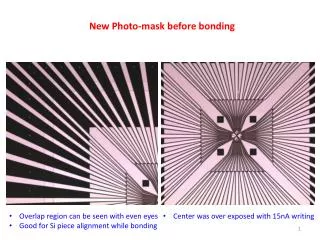
This document outlines the procedure and observations related to the photo-mask used before bonding silicon (Si) pieces. The overlap region is clearly visible, facilitating proper alignment during bonding. The center of the mask was deliberately overexposed at 15nA, ensuring that the silicon was firmly bonded. The metal stacking configurations for patterning include a titanum/nickel layer of 80nm/400nm for PL patterns and a multi-layered stack of 30nm Ti, 300nm Ni, 50nm Ti, and 100nm Ni for EBL patterns, designed to minimize total nickel consumption.

E N D
New Photo-mask before bonding • Overlap region can be seen with even eyes • Good for Si piece alignment while bonding • Center was over exposed with 15nA writing
Si was firmly bonded • Metal stacking for PL pattern: Ti/Ni=80nm/400nm • Metal stacking for EBL pattern: Ti/Ni/Ti/Ni=30nm/300nm/50nm/100nm (blocking total consumption of Ni)