Fetch Execute Cycle – In Detail -
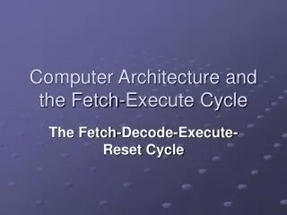
Fetch Execute Cycle – In Detail -. Simple Layout of Fetch-Execute Cycle. FETCH-EXECUTE CYCLE


Fetch Execute Cycle – In Detail -
E N D
Presentation Transcript
FETCH-EXECUTE CYCLE The fetch execute cycle is the time period of which the computer reads and processes the instructions from the memory, and executes them. This process is a continuous cycle which is used until the computer is turned off or there are no more instructions to process.
Fetch Cycle • Fetch the Instruction from Main Memory The CPU presents the value of the program counter on the address bus. The CPU then fetches the instruction from main memory via the data bus into the Instruction Register. • Decode the Instruction The instruction decoder (ID) interprets and implements the instruction Execute Cycle • Get Data from Main Memory Fetch required data from main memory to be processed and placed into registers. • Execute the Instruction Control signals are initialized to process the data using ALU and write the result back to a register. • Store Results The result generated by the operation is stored in the main memory, or sent to an output device.
As soon as a computer is powered on it begins the process of the fetch-execute cycle. • To do this it contains 4 main registries, • MBR (Memory Buffer Register) • MAR (Memory Address Register) • PC (Program Counter) • IR (Instruction Register).
Memory Buffer Register • This register has the job of storing the last collected data that has been fetched. If no fetch has occurred it contains the data from the last process. This then is the value the computer works with for the next instruction, or flushes it to memory (on command) to enable a new data to be stored. Memory Address Register • The memory address register contains the address of the memory of which we either want to read or write to. Program Counter • The program counter holds the address of the next instruction to be executed. Instruction Register • This holds the instruction for the last execution or, after fetch cycle has run and has moved onto the decode cycle, the current execution command.
How It Works? The fetch cycle • The fetch cycle collects the data from the memory and stores it in the MBR as well as setting the program to load the next step. This prepares the processor for the information is about to receive as well as progressing the program ready for the next processor cycle (the combination of all the cycles together). The following is the order for a fetch cycle. 1. Move PC to MAR: This progresses the program moving the 'next instruction' to be the current instruction. Progression starts here. 2. Move MAR to MBR: As MAR only holds an address of op code to be collected it is important that the data is now fetched into the processor buffer. 3. Increase PC: This sets the position of the next instruction to be executed. 4. Move MBR to IR: This allows the processor to now manipulate the buffer into operation code (op code) to be run by the processor. In some cases processors might be able to fetch more than one bit of data, supposing it has more than one buffer. If this is the case the process has to repeat to load each buffer. MBR (Memory Buffer Register), MAR (Memory Address Register), PC (Program Counter), IR (Instruction Register)
The Decode cycle • The decode cycle is responsible for fetching the memory the op code,fetched by the fetch cycle, needs. Depending on the op code this may take some time due, especially when fetching data from main memory. In this cycle it decodes indirect addresses (variable names) into direct addresses in the memory where the information is stored. The Execute cycle • This cycle processes the command and returns the result. An example would be the Assembler code Add R0, X. By this point R0 would have been translated into a proper address of where the data can be found by and collected. At this stage it would follow the following commands: 1. Move value at address X into MAR 2. Read the memory and insert value into MBR 3. Compute R0 added to the value of MBR and place in R0 MBR (Memory Buffer Register), MAR (Memory Address Register), PC (Program Counter), IR (Instruction Register)
The Interrupt cycle • This cycle would run to see if any other processes needed to run or were called by an event in a chip. These interrupts would be stored in another Register, separate from the cycle, so even if the system was half way through a cycle the interrupt would be noticed at this stage. The following would be executed to allow the execution of the new program and the successful save of the current. 1. Move current value of PC into MBR. 2. Move system stack address into MAR. 3. Move interrupt address into PC. 4. Move MBR into correct direct system stack address. 5. Continue cycle with new interrupt routine. 6. When finished return the system stack address loads and PC is obtained again. • Because the new process may be interrupted as well the system stack may fill up. As the processes end however they are removed from the stack and the program underneath is executed. The current running program is said to be at the top of the stack, and only the top of the system stack can be executed or dealt with. All others simply wait for the processor to finish the top process that interrupted. MBR (Memory Buffer Register), MAR (Memory Address Register), PC (Program Counter), IR (Instruction Register)
References • http://www.karbosguide.com/hardware/module5a3.htm • http://www.cs.mcgill.ca/~cs573/fall2003/suppnotes/lec273/lecture8/index.htm • http://en.wikipedia.org/wiki/Input/output_base_address