Interfacing The Serial/RS-232 Port
Interfacing The Serial/RS-232 Port . Hardware Serial Port Registers Programming. Interfacing the Serial / RS232 Port. The Serial Port is harder to interface than the Parallel Port. When receiving data and change in status from I/O Ports, two methods are available 1 . POLLING

Interfacing The Serial/RS-232 Port
E N D
Presentation Transcript
Interfacing The Serial/RS-232 Port Hardware Serial Port Registers Programming
Interfacing the Serial / RS232 Port The Serial Port is harder to interface than the Parallel Port.
When receiving data and change in status from I/O Ports, two methods are available • 1 . POLLING • Poll the port, which involves reading the status of the port at fixed intervals to determine whether any data has been received or a change of status has occurred. If so, then branch to a routine to service the ports requests. • 2 INTERRUPT HANDLING • when a I/O Port/Device needs attention as a byte has been received or status has changed, then it sends a Interrupt Request (IRQ) to the processor. • Once the processor receives an Interrupt Request, it finishes its current instruction, places a few things on the stack, and executes the appropriate Interrupt Service Routine (ISR) which can remove the byte from the port and place it in a buffer. Once the ISR has finished, the processor returns to where it left off.
Hardware Interrupts • The Programmable Interrupt Controller (PIC) handles hardware interrupts. • Most PC's will have two of them located at different addresses. • One handles IRQ's 0 to 7 and the other, IRQ's 8 to 15, giving a total of 15 individual IRQ lines • The first PIC, located at Base Address 0x20h controls IRQ 0 to IRQ 7. • The second PIC located at a base address of 0xA0h controls IRQs 8 to 15.
Bit Disable IRQ Function 7 IRQ7 Parallel Port 6 IRQ6 Floppy Disk Controller 5 IRQ5 Reserved/Sound Card 4 IRQ4 Serial Port 3 IRQ3 Serial Port 2 IRQ2 PIC2 1 IRQ1 Keyboard 0 IRQ0 System Timer • . PIC1 (0x21) outportb(0x21,(inportb(0x21) & 0xF7); to enable IRQ3. outportb(0x21,(inportb(0x21) | 0x08); used to disable IRQ3
End of Interrupt (EOI): This is sent to the PIC at the end of the Interrupt Service Routine so that the PIC can reset the In Service Register. An EOI can be sent using outportb(0x20,0x20); for PIC1 or outportb(0xA0,0x20); for PIC2 • PIC2 (0xA1) Bit Disable IRQ Function 7 IRQ15 Reserved 6 IRQ14 Hard Disk Drive 5 IRQ13 Maths Co-Processor 4 IRQ12 PS/2 Mouse 3 IRQ11 Reserved 2 IRQ10 Reserved 1 IRQ9 Redirected IRQ2 0 IRQ8 Real Time Clock
any device connected to the serial port will need the serial transmission converted back to parallel so that it can be used • This can be done using a UART • Devices which use serial cables for their communication are split into two categories. • DCE (Data Communications Equipment) • DTE (Data Terminal Equipment.) • Data Communications Equipment are devices such as • modem, TA adapter, plotter etc while Data • Terminal Equipment is Computer or Terminal.
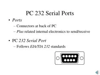
Serial Ports come in two "sizes" • There are the D-Type 25 pin connector and the • D-Type 9 pin connector
Pin Functions AbbreviationFull NameFunction TDTransmit DataSerial Data Output (TXD) RDReceive DataSerial Data Input (RXD) CTSClear to SendThis line indicates that theModem is ready toexchange data. DCDData Carrier DetectWhen the modem detects a "Carrier" from the modem atthe other end ofthephoneline, this Linebecomes active. DSRData Set ReadyThis tells the UART that the modem is ready to establish alink.
AbbreviationFull NameFunction DTRData Terminal ReadyThis is the opposite to DSR. Thistells the Modem that the UARTis ready to link. RTSRequest To SendThis line informs the Modem that the UART is ready toexchangedata. RIRing IndicatorGoes active when modem detects a ringing signal from the PSTN.
NULL MODEMS • A Null Modem is used to connect two DTE's together.
Above is method of wiring Null Modem • It only requires 3 wires (TD, RD & SG) to be wired. • Null Modems make to computer think it is talking to a modem rather than another computer. • Any data transmitted from the first computer must be received by the second thus TD is connected to RD. The second computer must have the same set-up thus RD is connected to TD. • Signal Ground (SG) must also be connected so both grounds are common to each computer. • The Data Terminal Ready is looped back to Data Set Ready and Carrier Detect on both computers. • When the Data Terminal Ready is asserted active, then the Data Set Ready and Carrier Detect immediately become active. At this point the computer thinks the Virtual Modem to which it is connected is ready and has detected the carrier of the other modem.
Request to Send and Clear To Send, As both computers communicate together at the same speed, flow control is not needed thus these two lines are also linked together on each computer. • When the computer wishes to send data, it asserts the Request to Send high and as it's hooked together with the Clear to Send, It immediately gets a reply that it is ok to send and does so. • Line RTS tells the Modem that UART is ready to exchange data, and the loop back to the line CTS indicate that the Modem is ready to excahange data. • When the DTR is set ,which tells the modem that UART is ready to make link & this signal is looped back to DSR , which tells UART that modem is ready to make link & carrier detect tells modem that the other end of the line is active.
Flow Control • Sooner or later data is going to get lost as buffers overflow, thus flow control is used. Flow control has two basic varieties, • Hardware or Software. • Software flow control, sometimes expressed as Xon/Xoff uses two characters Xon and Xoff. • Xon is normally indicated by the ASCII 17 character where as the ASCII 19 character is used for Xoff. • when the computer fills the buffer of modem, the modem sends a Xoff character to tell the computer to stop sending data. • Once the modem has room for more data it then sends a Xon character and the computer sends more data.
Hardware flow control is also known as RTS/CTS flow control. • It uses two wires in serial cable rather than extra characters transmitted in data lines. • Thus hardware flow control will not slow down transmission times like Xon-Xoff does. • When the computer wishes to send data it takes active the Request to Send line. If the modem has room for this data, then the modem will reply by taking active the Clear to Send line and the computer starts sending data. If the modem does not have the room then it will not send a Clear to Send.
THE UART • UART stands for Universal Asynchronous Receiver / Transmitter. • The 8250 series, which includes the 16450, 16550, 16650, & 16750 UARTS are the most commonly found type in your PC. • It’s is usually integrated with serial cards.
The 16550 introduced two new pins at 24 and 29. • These are Transmit Ready at 24 and Receive Ready at 29 which can be implemented with DMA (Direct Memory Access). • These Pins have two different modes of operation. • Mode 0 supports single transfer DMA where as Mode 1 supports Multi-transfer DMA. • Mode 0 is also called the 16450 mode. • This mode is selected when the FIFO buffers are disabled via Bit 0 of the FIFO Control Register or When the FIFO buffers are enabled but DMA Mode Select = 0. • (Bit 3 of FCR) In this mode RXRDY is active low when at least one character (Byte) is present in the Receiver Buffer. • . RXRDY will go inactive high when no more characters are left in the Receiver Buffer.
TXRDY will be active low when there are no characters in the Transmit Buffer. • It will go inactive high after the first character / byte is loaded into the Transmit Buffer. • *later*
Name Address IRQ COM 1 3F8 4 COM 2 2F8 3 COM 3 3E8 4 COM 4 2E8 3 Serial Port's Registers Port Addresses & IRQ's Above are the standard port addresses.
Start Address Function 0000:0400 COM1's Base Address 0000:0402 COM2's Base Address 0000:0404 COM3's Base Address 0000:0406 COM4's Base Address The above table shows the address at which we can find the Communications (COM) ports addresses in the BIOS Data Area. Each address will take up 2 bytes.
#include <stdio.h> #include <dos.h> void main(void) { unsigned int far *ptraddr; /* Pointer to location of Port Addresses*/ unsigned int address; /* Address of Port */ int a; ptraddr=(unsigned int far *)0x00000400; for (a = 0; a < 4; a++) { address = *ptraddr; if (address == 0) printf("No port found for COM%d \n",a+1); else printf("Address assigned to COM%d is %Xh\n",a+1,address); *ptraddr++; } }
REGISTERS 12 registers Through only 8 port addresses Table of Registers
Base Address DLAB Read/Write Abr. Register Name + 0 =0 Write - Transmitter Holding Buffer =0 Read - Receiver Buffer =1 Read/Write - Divisor Latch Low Byte + 1 =0 Read/Write IER Interrupt Enable Register =1 Read/Write - Divisor Latch High Byte + 2 - Read IIR Interrupt Identification Register - Write FCR FIFO Control Register + 3 - Read/Write LCR Line Control Register + 4 - Read/Write MCR Modem Control Register + 5 - Read LSR Line Status Register + 6 - Read MSR Modem Status Register + 7 - Read/Write - Scratch Register Table 5 : Table of Registers
When DLAB is set to '0' or '1' some of the registers change. • This is how the UART is able to have 12 registers (including the scratch register) through only 8 port addresses. • DLAB stands for Divisor Latch Access Bit. • . When DLAB is set to '1' via the line control register, two registers become available from which we can set your speed of communications measured in bits per second. • the UART is fitted with a Programmable Baud Rate Generator which is controlled by these two registers. • The first register (Base + 0) when DLAB = 1 stores the "Divisor latch low byte" where as the second register (base + 1 when DLAB = 1) stores the "Divisor latch high byte.“
Speed (BPS) Divisor (Dec) Divisor Latch High Byte Divisor Latch Low Byte 50 2304 09h 00h 300 384 01h 80h 600 192 00h C0h 2400 48 00h 30h 4800 24 00h 18h 9600 12 00h 0Ch 19200 6 00h 06h 38400 3 00h 03h 57600 2 00h 02h 115200 1 00h 01h
Bit Notes Bit 7 Reserved Bit 6 Reserved Bit 5 Enables Low Power Mode (16750) Bit 4 Enables Sleep Mode (16750) Bit 3 Enable Modem Status Interrupt Bit 2 Enable Receiver Line Status Interrupt Bit 1 Enable Transmitter Holding Register Empty Interrupt Bit 0 Enable Received Data Available Interrupt Interrupt Enable Register(IER) :
Read/Write Register • DLAB=0 • Setting Bit 0 high enables the Received Data Available Interrupt which generates an interrupt when the receiving register/FIFO contains data to be read by the CPU. • Bit 1 enables Transmit Holding Register Empty Interrupt. This interrupts the CPU when the transmitter buffer is empty. • Bit 2 enables the receiver line status interrupt. The UART will interrupt when the receiver line status changes. • Likewise for bit 3 which enables the modem status interrupt.
Interrupt Identification Register(IIR) Table of IIR
Bit Notes Bits 6 and 7 Bit 6 Bit 7 0 0 No FIFO 0 1 FIFO Enabled but Unusable 1 1 FIFO Enabled Bit 5 64 Byte Fifo Enabled (16750 only) Bit 4 Reserved Bit 3 0 Reserved on 8250, 16450 1 16550 Time-out Interrupt Pending Bits 1 and 2 Bit 2 Bit 1 0 0 Modem Status Interrupt 0 1 Transmitter Holding Register Empty Interrupt 1 0 Received Data Available Interrupt 1 1 Receiver Line Status Interrupt Bit 0 0 Interrupt Pending 1 No Interrupt Pending
Read only register • Bits 6 and 7 give status on the FIFO Buffer. • Bit 0 which shows whether an interrupt has occurred. If an interrupt has occurred it's status will shown by bits 1 and 2.
FIRST IN / FIRST OUT Control Register ( FCR ) Table of FCR
Bit Notes Bits 6 and 7 Bit 7 Bit 6 Interrupt Trigger Level 0 0 1 Byte 0 1 4 Bytes 1 0 8 Bytes 1 1 14 Bytes Bit 5 Enable 64 Byte FIFO (16750 only) Bit 4 Reserved Bit 3 DMA Mode Select. Change status of RXRDY & TXRDY pins from mode 1 to mode 2. Bit 2 Clear Transmit FIFO Bit 1 Clear Receive FIFO Bit 0 Enable FIFO's
The FIFO register is a write only register. • Bit 0 enables the operation of the receive and transmit FIFO's. • Writing a '0' to this bit will disable the operation of transmit and receive FIFO's, thus you will loose all data stored in these FIFO buffers. • Bit's 1 and 2 control the clearing of the transmit or receive FIFO's. • Bits 6 and 7 are used to set the triggering level on the Receive FIFO. • For example if bit 7 was set to '1' and bit 6 was set to '0' then the trigger level is set to 8 bytes. When there is 8 bytes of data in the receive FIFO then the Received Data Available interrupt is set. See (IIR)
LINE CONTROL REGISTER (LCR) Table
Bit 7 1 Divisor Latch Access Bit 0 Access to Receiver buffer, Transmitter buffer & Interrupt Enable Register Bit 6 Set Break Enable Bits 3, 4 And 5 Bit 5 Bit 4 Bit 3 Parity Select X X 0 No Parity 0 0 1 Odd Parity 0 1 1 Even Parity 1 0 1 High Parity (Sticky) 1 1 1 Low Parity (Sticky) Bit 2 Length of Stop Bit 0 One Stop Bit 1 2 Stop bits for words of length 6,7 or 8 bits or 1.5 Stop Bits for Word lengths of 5 bits. Bits 0 And 1 Bit 1 Bit 0 Word Length 0 0 5 Bits 0 1 6 Bits 1 0 7 Bits 1 1 8 Bits
The Line Control register sets the basic parameters for communication. • Bit 7 is the Divisor Latch Access Bit or DLAB for short. • Bits 3,4 and 5 select parity, bit 3 controls parity. • Bit 2 sets the length of the stop bits. Setting this bit to '0' will produce one stop bit. • Bits 0 and 1 set the word length.
Modem Control Register (MCR) Bit Notes Bit 7 Reserved Bit 6 Reserved Bit 5 Autoflow Control Enabled (16750 only) Bit 4 LoopBack Mode Bit 3 Aux Output 2 Bit 2 Aux Output 1 Bit 1 Force Request to Send Bit 0 Force Data Terminal Ready • The Modem Control Register is a Read/Write Register
Line Status Register (LSR) Bit Notes Bit 7 Error in Received FIFO Bit 6 Empty Data Holding Registers Bit 5 Empty Transmitter Holding Register Bit 4 Break Interrupt Bit 3 Framing Error Bit 2 Parity Error Bit 1 Overrun Error Bit 0 Data Ready
The line status register is a read only register. • Bit 7 is the error in received FIFO bit. • Bit 0 shows data ready, which means that a byte has been received by the UART and is at the receiver buffer ready to be read
Modem Status Register (MSR) Bit Notes Bit 7 Carrier Detect Bit 6 Ring Indicator Bit 5 Data Set Ready Bit 4 Clear To Send Bit 3 Delta Data Carrier Detect Bit 2 Trailing Edge Ring Indicator Bit 1 Delta Data Set Ready Bit 0 Delta Clear to Send
Bit 0 of the modem status register shows delta clear to send. • delta meaning a change in, thus delta clear to send means that there was a change in the clear to send line, since the last read of this register. • This is the same for bits 1 and 3. • Bits 4 to 7 show the current state of the data lines when read.