Solution: R-2R Ladder
500 likes | 789 Vues
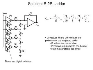
Solution: R-2R Ladder. V out. Using just R and 2R removes the problems of the weighted adder R values are reasonable Precision requirements can be met RC time constants are small. These are digital switches. R-2R Ladder: Thevenin analysis.

Solution: R-2R Ladder
E N D
Presentation Transcript
Solution: R-2R Ladder Vout • Using just R and 2R removes the problems of the weighted adder • R values are reasonable • Precision requirements can be met • RC time constants are small These are digital switches
R-2R Ladder: Thevenin analysis How do we end up with these weights? Apply Thevenin's...
Announcements • Assignment 8 posted • Due Tomorrow. A bit longer than others. • Project progress? • Dates • Tuesday 12/6 project demonstrations in the lab (no presentations) • Sunday 12/11 project reports due to me by email • Tuesday 12/13 final exam, 1pm-3pm here.
Lecture 25: Review • Exam preparation – use assignments, go over the mid-term (solutions posted on Assignments page). Use this review. Practice with EWB • Can’t review everything – focus on some older stuff today • Simple circuits: equivalent circuits (work for both AC & DC) • KCL KVL; mesh or nodal analysis. Works for AC & DC • Thevenin & Norton circuits • Transient circuits; capacitors & inductors • These notes contain (much) more, and will be posted on the web
Simple circuits • Voltage/Current sources: provide prescribed voltage/current regardless of load • Kirchoff's current law: The sum of currents into a node=0 • Kirchoff's Voltage Law: The sum of voltages round a closed loop=0 • Voltage divider: • Current divider
Circuit analysis method 1:Apply element combination rules Series resistors Parallel resistors Series voltage sources Parallel current sources
Mesh Analysis • Example: 2 meshes • (Mesh is a loop that does not contain other loops) • Step 1: Assign mesh currents clockwise • Step 2: Apply KVL to each mesh • The self-resistance is the effective resistance of the resistors in series within a mesh. The mutual resistance is the resistance that the mesh has in common with the neighbouring mesh • To write the mesh equation, evaluate the self-resistance, then multiply by the mesh current • Next, subtract the mutual resistance multiplied by the current in the neighbouring mesh for each neighbour. • Equate the above result to the driving voltage: taken to be positive if it tends to push current in the same direction as the assigned mesh current Mesh1: (R1+R2)I1 - R2I2 =ε1-ε2 Mesh2: -R2I1+ (R2+R3)I2 =ε2-ε3 Step 3: solve currents: use substitution or Cramer's rule
Cramer's Rule Step 3: solve currents: use substitution or Cramer's rule PRACTICE!!!http://sole.ooz.ie/en I - I2 - I3 = 0 4I + 5I2 + 0I3= 3 0I - 5I2 + 10I3= 0
Mesh analysis with a current source Magnitude of current in mesh containing current source is IS, (although if the current flow is opposite to the assigned current direction the value will be negative). This works only if the current source is not shared by any other mesh For a shared current source, label it with an unknown voltage.
Example • In this circuit, find the value of Is that will reduce the voltage across the 4Ω resistor to zero.
Example • In this circuit, find the value of Is that will reduce the voltage across the 4Ω resistor to zero. Mesh equation: when 4Ω voltage=0: • What if the 2 Ω and the 6 Ω resistors are swapped?
Example II • Which of the two circuits has the larger terminal voltage, A or B? • Which has the larger current through the 9V battery? • Practical batteries are modelled as voltage sources in series with a resistor.
Example II • Which of the two circuits has the larger terminal voltage, A or B? • Which has the larger current through the 9V battery? • Practical batteries are modelled as voltage sources in series with a resistor. Mesh equations: Mesh equations: i1= current through 9V battery solve to give i1=0.41A i1 = current through 9V battery solve to give i1= -0.56A
Example II • Which of the two circuits has the larger terminal voltage, A or B? • Which has the larger current through the 9V battery? • Practical batteries are modelled as voltage sources in series with a resistor. x x + + VR - - i1 - i1 - VR + + y y i1= current through battery solve to give i1=0.41A i1 = current through battery solve to give i1= -0.56A
Thevenin and Norton Equivalent Circuits Any network of sources and resistors will appear to the circuit connected to it as a single voltage source and a series resistance load vTH= open circuit voltage at terminal (a.k.a. port) RTH= Resistance of the network as seen from port (Vm’s, In’s set to zero) load
Thevenin and Norton Equivalent Circuits Any network of sources and resistors will appear to the circuit connected to it as a single current source and a parallel resistance How do we calculate RT, VT, iN, RN ?
Calculation of RT and RN • RT=RN ; same calculation • Set all sources to zero (‘kill’ the sources) • Short voltage sources • Open Current sources • Calculate equivalent resistance seen by the load
Calculation of VT • Remove the load and calculate the open circuit voltage • The Thevenin equivalent is then VT in series with RT
Example • Find the Thevenin equivalent
Example • Find the Thevenin equivalent
Example • Find the Thevenin equivalent Y X X Y
AC circuit elements • Capacitors in series: • Capacitors in parallel: • Capacitive impedance: ZC=1/jωC • Inductors in series: • Inductors in parallel: • Inductive impedance: ZL= jωL • Circuit analysis tools for DC circuits work on AC circuits, but replace resistance with complex impedance
AC circuit analysis example If V1=10cos(1000t) (volts)and V2=5cos(1000t) (volts), what is the current through the capacitor?
AC circuit analysis example If V1=10cos(1000t) (volts)and V2=5cos(1000t) (volts), what is the current through the capacitor? Mesh 1: (100+ZC)I1-ZCI2=V1 Mesh 2: -ZcI1+(Zc+ZL)I2=-V2 IC(jω)=I1(jω)-I2(jω)=0.05j+0.05+0.05j=0.05+0.1j φ=tan-1(0.1/0.05) = 63 degrees A=√(0.052+0.12)=0.11 IC(jω)=0.1163 iC(t)=0.11cos(1000t+63)
0.37 Charging a capacitor Time constant τ=RC. Time needed to charge capacitor to 63% of full charge Larger RC means the capacitor takes longer to charge Larger R implies smaller current flow The larger C is, the more charge the capacitor can hold. Solution is only true for simple circuit with resistor and capacitor in series, but more complicated circuits can be reduced to this using Thevenin's Theorem
Example A battery with an emf of 1.5V and an internal resistance of 0.6Ω is used to charge a 5F capacitor when a switch is closed. How long does it take to reach a voltage across the capacitor of 1V? 5F
Example A battery with an emf of 1.5V and an internal resistance of 0.6Ω is used to charge a 5F capacitor when a switch is closed. How long does it take to reach a voltage across the capacitor of 1V? 5F
Example How long does it take if we attach an additional battery with an emf of 9V and an internal resistance of 18Ω as shown? 5F
Example How long does it take if we attach an additional battery with an emf of 9V and an internal resistance of 18Ω as shown? RTH=0.58 Ohm i= 0.40 A VTH=1.74 V 5F Time to 1V= 2.5 seconds 5F
Op Amps Remember the Golden Rules: 1) iin=0: no current flows into the opamp. 2) v+=v- These are only valid when there is negative feedback In many circuits, one input to the opamp is connected to ground, so v+=v-=0 A simple example:
Op Amp circuits Summing Amplifier Inverting Amplifier Non-Inverting Amplifier Differential Amplifier
Integrator Differentiator And two without negative feedback: Schmitt Trigger Comparator
Example What does this circuit do? Derive an expression for the gain and give the circuit a suitable name. i2 R2 i1 R1 R1 R1=R2 R2 voltage divider
Example Design an opamp circuit to convert the triangular waveform v1 in the following figure into the square wave v0 shown. Use a 0.1μF capacitor. (Hint: first quantitatively determine the mathematical expression of v0 in terms of v1) v0 is v1 differentiated
Simple Filter analysis: Which of the following is a low-pass filter? • What happens to the output voltage when ω→0 (DC condition)? • In DC circuits, capacitors are open, inductors are shorts. • or when ω→∞ • At very high frequencies, capacitors are shorts, inductors are open Answer: (c)
For a more quantitative solution, find the complex transfer function: • RC low-pass filter: preserves lower frequencies, attenuates frequencies above the 3dB cutoff frequency ω0=1/RC. (For voltage)
Example Design a high-pass RC filter with a 3dB frequency cutoff of 80Hz using a capacitor of 2μF
Example Given an input signal Vi=10mV(sin10t+sin10,000t), design a circuit such that the output signal is VO= -100mV(sin10t). The high frequency component of the output signal must be <1% of the low frequency part. So, we want a circuit which amplifies the voltage, but only at low frequencies: need an active filter.
Example Given an input signal Vi=10mV(sin10t+sin10,000t), design a circuit such that the output signal is VO= -100mV(sin10t). The high frequency component of the output signal must be <1% of the low frequency part. So, we want a circuit which amplifies the voltage, but only at low frequencies: need an active filter. Low frequency ω1: Want a gain of 10 ω1RFCF<<1 so set RS=1kΩ set RF=10kΩ High frequency ω2: Low frequency gain=10, so for <1%, need high frequency gain <1/10 Check low frequency:
Combinational logic design steps: • Derive the Truth Table • Fill the Karnaugh map • Use the map to find the logic • Implement the logic in a circuit
Another Example: 7 segment displays Karnaugh Map for "a" Truth Table "x" represents a "don't care" condition - the value can be either 0 or 1
Box the ones for sum-of-products This subcube: A·C • This subcube: B This subcube: A'·C' This subcube: D
Sequential logic design steps: • List the states - assign each state a symbol • Draw the finite state diagram (Moore - states inside nodes) • Derive the symbolic state transition table • Assign each state a binary code (also each output, if more than one) • Derive the actual state transition table • Write out the Karnaugh map for each "next state" and output(s) • Solve the maps to find the logic • Implement the logic in a circuit
current state next state0 000 001 11 001 010 22 010 011 33 011 100 44 100 101 55 101 110 66 110 111 77 111 000 0 010 011 001 1 2 3 000 100 3-bit up-counter 4 0 110 101 111 7 6 5 3-bit binary up-counter: List the states: 0 to 7 Derive the symbolic transition table Draw the finite state diagram
current state next state0 000 001 11 001 010 22 010 011 33 011 100 44 100 101 55 101 110 66 110 111 77 111 000 0 010 011 001 000 100 3-bit up-counter 110 101 111 Derive the actual state transition table Assign the states a binary code
C3 C3 0 1 1 0 1 1 0 0 1 0 0 1 1 1 0 0 C1 C1 C2 C2 C3 C2 C1 N3 N2 N10 0 0 0 0 10 0 1 0 1 00 1 0 0 1 10 1 1 1 0 01 0 0 1 0 11 0 1 1 1 01 1 0 1 1 11 1 1 0 0 0 N1 N2 N3 C3 C3C2 00 01 11 10 C1 0 0 0 0 1 1 1 0 1 1 C1 C2 Derive the actual state transition table current next Solve the maps notation to show function representing input to D-FF N1 := C1' N2 := C1C2' + C1'C2 := C1 xor C2 N3 := C1C2C3' + C1'C3 + C2'C3 := C1C2C3' + (C1' + C2')C3 := C1C2C3' + (C1C2)'C3 := (C1C2) xor C3 Karnaugh maps for each "next state":
C3 C2 C1 N3 N2 N10 0 0 0 0 10 0 1 0 1 00 1 0 0 1 10 1 1 1 0 01 0 0 1 0 11 0 1 1 1 01 1 0 1 1 11 1 1 0 0 0C3 C2 C1 N3 N2 N10 0 0 0 0 10 0 1 0 1 00 1 0 0 1 10 1 1 1 0 01 0 0 1 0 11 0 1 1 1 01 1 0 1 1 11 1 1 0 0 0 Implement the logic: each state bit requires one memory element (flipflop) current next N1 := C1' N2 := C1C2' + C1'C2 := C1 xor C2 N3 := C1C2C3' + C1'C3 + C2'C3 := C1C2C3' + (C1' + C2')C3 := (C1C2) xor C3