Download
1 / 29
340 likes | 632 Vues
MODES OF 8086. Details of Pins. Pin 1 –Connected Ground Pins 2-16 –acts as both input/output . Outputs address at the first part of the cycle and outputs or inputs data in the remaining part of the cycle Pin 17- Non maskable interrupt Pin 18-INTR- maskable interrupt request

E N D
Details of Pins • Pin 1 –Connected Ground • Pins 2-16 –acts as both input/output . Outputs address at the first part of the cycle and outputs or inputs data in the remaining part of the cycle • Pin 17- Non maskable interrupt • Pin 18-INTR- maskable interrupt request • Pin -19-CLK- 5MHz for 8086 • Pin -20-connected Ground • Pin 21- RESET- Terminating activity. A high(1) on this pin clears IP,CS, DS, SS, ES and instruction queue cleared and CS set to FFFF. With IP=000 and CS=FFFF, the processor will begin executing at FFFF0.
This location is a read-only location in memory and contains jmp instruction to a program for initializing the system. • This program is called as Bootstrap loader. • Pin 22-READY – this pin will receive a ack from a memory or I/O interface that i/p data will be put on the bus or o/p data will be accepted from the data bus in the next clk cycle. • Pin 23-TEST-Used in conjunction with WAIT inst in multiprocessing environment. • Pin 24-31- are mode dependent- will be explained with each mode. • Pin-32-RD indicates that i/p operation has to be performed. • Pins 33- indicates current mode of the CPU. Processor is in minimum mode if connected to +5V and in maximum mode if connected to ground.
Pin-34 If connected to ground during the first part of the bus cycle, then it means that at least one byte of the current transfer is to be made on pins AD8-AD15. if high, then transfer is made on AD0-AD7. Together with BHE and A0 signals indicate how data appear on the bus. The four possible combinations are:
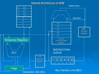
Pins 35-38 During the first part of the bus cycle, the upper 4 bits of the address are o/p and during the remainder of the bus cycle, these status mentioned below is the is o/p. S4 S3 Register 0 0 ES 0 1 SS 1 0 CS 1 1 DS S5 gives the current setting of IF S6 is always 0, indicates 8086 controlling the bus. Pin-39 AD15- same as AD0-AD14(ie pins 2-16) Pin-40-VCC connected to +5V
Minimum Mode • The minimum mode is used for a small system with a single processor, a system in which the 8086 alone generates all the possible control signals directly. • The 8086 processor is in minimum mode when pin 33(MN/MX) is given +5V. • The definitions for pins 24 through 31 for the minimum mode are as follows. • Pin-24-INTA Indicates recognition of an interrupt request. • Pin 25-ALE -o/p a pulse indicating that address is available on address pins • Pin-26-DEN This is to inform the transceivers that CPU is ready to send or receive data.
Pin-27 DT/R Indicates transceivers whether they are to transmit(1) or receive(0) data. • Pin-28 M/IO Distinguishes a memory transfer from an I/O transfer. For a memory transfer it is 1. • Pin-29 WR it is used to indicate write operation. It is used with conjunction with pin 28 to indicate type of transfer. • Pin 30 HLDA outputs a bus grant signal to a requesting master • Pin 31 HOLD Receives bus request from bus masters
Minimum mode system • The address must be latched since it is available only during first part of the bus cycle. • To signal that address is ready to be latched, 1 is put on pin 25(ALE). • Since 8282 is 8-bit latch , 2 or 3 8282 latches are needed to implement full 20-bit address. • 8286 –transceiver device. It contains 8 receivers and drivers. So for an 8086 it needs two 8286. • When OE(active low) is high, data are not transmitted through 8286 in either direction. • If it is low and T=1, then they have to act as transmitters of data and if T=0, then they have to receive data.
We have 8284A clock generator. This device is more than just a clock generator. In addition to supplying a train of pulses at a constant frequency, it synchronizes ready(RDY) signals, which indicate an interface is ready to complete a transfer and reset(RES(active low)) which initializes the system with clock pulse. • All these three devices 8282, 8286 and 8284A require +5V supply. • In a minimum mode system control lines need not pass through transceivers, but directly used
The M/IO, RD and WR lines specify the type of transfer. M/IO RD WR 0 0 1 I/O read 0 1 0 I/O write 1 0 1 memory read 1 1 0 memory write
Maximum Mode • A processor is in maximum mode, if MN/MX pin is grounded. • This mode provides signals for implementing multiprocessor systems and Co-processor system environment. • The difference between minimum and maximum mode configurations is the need for additional circuitry to translate the control signals. • This circuitry is for converting the status bits S0, S1, and S2 into the I/O and memory transfer signals needed to direct data transfer. It is normally implemented by Intel 8288 bus controller. • Also included in this system is interrupt priority controller. However its presence is optional.
Pins 24-25 QS1 QS2 Reflects the status of the instruction queue. This Status indicates the activity in the queue during the previous clock cycle.
Pins 26-28- S0,S1, S2- Indicates type of transfer to take place during current bus cycle.
Pin 29 Indicates that bus is not be relinquished to other potential bus masters • Pin 30 RQ/GT1 for inputting bus request and outputting bus grant signals. • Pin 31 RQ/GT0 same as pin 30 except that a request on this pin has higher priority. • The basic function of the bus controller chip IC8288, is to derive control signals like RD and WR ( for memory and I/O devices), DEN, DT/R, ALE etc. using the information by the processor on the status lines. • The bus controller chip has input lines S2, S1, S0 and CLK. These inputs to 8288 are driven by CPU. • It derives the outputs ALE, DEN, DT/R, MRDC, MWTC, AMWC, IORC, IOWC and AIOWC.
![8086 [2]](https://cdn1.slideserve.com/2457127/8086-2-dt.jpg)