Download
1 / 46
510 likes | 895 Vues
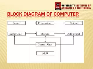
Explore the block diagram, registers, and control signals of the 8086 microprocessor software model. Learn about the various purpose registers, stack operations, and interrupt handling. Understand the coprocessor and multiprocessor configurations in the 8086 system.

E N D
General Purpose Registers • Normally used for storing temporary results • Each of the registers is 16 bits wide (AX, BX, CX, DX) • Can be accessed as either 16 or 8 bits AX, AH, AL • AX - the Accumulator • BX - the Base Register • CX - the Count Register • DX - the Data Register
General Purpose Registers • AX • Accumulator Register • Preferred register to use in arithmetic, logic and data transfer instructions because it generates the shortest Machine Language Code • Must be used in multiplication and division operations • Must also be used in I/O operations • BX • Base Register • Also serves as an address register
General Purpose Registers • CX • Count register • Used as a loop counter • Used in shift and rotate operations • DX • Data register • Used in multiplication and division • Also used in I/O operations
Pointer and Index Registers • All 16 bits wide, L/H bytes are not accessible • Used as memory pointers • Example: MOV AH, [SI] • Move the byte stored in memory location whose addressis contained in register SI to register AH • IP is not under direct control of the programmer
Flag Register Overflow Carry Direction Parity Auxiliary Carry Interrupt enable Trap Zero 6 are status flags 3 are control flag Sign
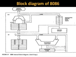
8086 Programmer’s Model ES Extra Segment CS Code Segment BIU registers (20 bit adder) SS Stack Segment DS Data Segment IP Instruction Pointer EU registers AX AH AL Accumulator BX BH BL Base Register CX CH CL Count Register DX DH DL Data Register SP Stack Pointer BP Base Pointer Source Index Register SI DI Destination Index Register FLAGS
The Stack • The stack is used for temporary storage of information such as data or addresses. • When a CALL is executed, the 8086 automatically PUSHes the current value of CS and IP onto the stack. • Other registers can also be pushed • Before return from the subroutine, POP instructions can be used to pop values back from the stack into the corresponding registers.
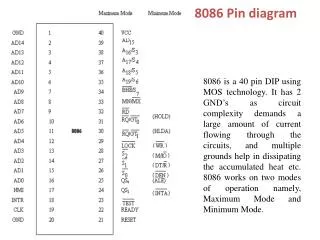
INTEL 8086 - Pin Details Power Supply 5V 10% Ground Reset Registers, seg regs, flags CS: FFFFH, IP: 0000H If high for minimum 4 clks Clock Duty cycle: 33%
INTEL 8086 - Pin Details Address/Data Bus: Contains address bits A15-A0 when ALE is 1 & data bits D15 – D0 when ALE is 0. Address Latch Enable: When high, multiplexed address/data bus contains address information.
INTEL 8086 - Pin Details INTERRUPT Non - maskable interrupt Interrupt acknowledge Interrupt request
INTEL 8086 - Pin Details Direct Memory Access Hold Hold acknowledge
INTEL 8086 - Pin Details Address/Status Bus Address bits A19 – A16 & Status bits S6 – S3
INTEL 8086 - Pin Details BHE#, A0: 0,0: Whole word (16-bits) 0,1: High byte to/from odd address 1,0: Low byte to/from even address 1,1: No selection Bus High Enable/S7 Enables most significant data bits D15 – D8 during read or write operation. S7: Always 1.
INTEL 8086 - Pin Details Min/Max mode Minimum Mode: +5V Maximum Mode: 0V Minimum Mode Pins Maximum Mode Pins
Read Signal Write Signal Memory or I/0 Data Transmit/Receive Data Bus Enable Minimum Mode- Pin Details
Maximum Mode - Pin Details S2 S1 S0 000: INTA 001: read I/O port 010: write I/O port 011: halt 100: code access 101: read memory 110: write memory 111: none -passive Status Signal Inputs to 8288 to generate eliminated signals due to max mode.
Maximum Mode - Pin Details Lock Output Used to lock peripherals off the system Activated by using the LOCK: prefix on any instruction DMA Request/Grant Lock Output
Maximum Mode - Pin Details QS1 QS0 00: Queue is idle 01: First byte of opcode 10: Queue is empty 11: Subsequent byte of opcode Queue Status Used by numeric coprocessor (8087)
Maximum Mode 8086 System • Here, either a numeric coprocessor of the type 8087 or another processor is interfaced with 8086. • The Memory, Address Bus, Data Buses are shared resources between the two processors. • The control signals for Maximum mode of operation are generated by the Bus Controller chip 8788. • The three status outputs S0*, S1*, S2* from the processor are input to 8788. • The outputs of the bus controller are the Control Signals, namely DEN, DT/R*, IORC*, IOWTC*, MWTC*, MRDC*, ALE etc.
8086 Control Signals • ALE • BHE • M/IO • DT/R • RD • WR • DEN
Coprocessor and Multiprocessor configuration • Multiprocessor Systems refer to the use of multiple processors that executes instructions simultaneously and communicate with each other using mail boxes and Semaphores. • Maximum mode of 8086 is designed to implement 3 basic multiprocessor configurations: 1. Coprocessor (8087) 2. Closely coupled (8089) 3. Loosely coupled (Multibus)
Coprocessor and Multiprocessor configuration • Coprocessors and Closely coupled configurations are similar in that both the 8086 and the external processor shares the: - Memory - I/O system - Bus & bus control logic - Clock generator
TEST pin of 8086 • Used in conjunction with the WAIT instruction in multiprocessing environments. • This is input from the 8087 coprocessor. • During execution of a wait instruction, the CPU checks this signal. • If it is low, execution of the signal will continue; if not, it will stop executing.
Coprocessor Execution Example Coprocessor cannot take control of the bus, it does everything through the CPU
Closely Coupled Execution Example • Closely Coupled processor may take control of the bus independently. • Two 8086’s cannot be closely coupled.
Loosely Coupled Configuration • has shared system bus, system memory, and system I/O. • each processor has its own clock as well as its own memory (in addition to access to the system resources). • Used for medium to large multiprocessor systems. • Each module is capable of being the bus master. • Any module could be a processor capable of being a bus master, a coprocessor configuration or a closely coupled configuration.
Loosely Coupled Configuration • No direct connections between the modules. • Each share the system bus and communicate through shared resources. • Processor in their separate modules can simultaneously access their private subsystems through their local busses, and perform their local data references and instruction fetches independently. This results in improved degree of concurrent processing. • Excellent for real time applications, as separate modules can be assigned specialized tasks
Advantages of Multiprocessor Configuration • High system throughput can be achieved by having more than one CPU. • The system can be expanded in modular form. Each bus master module is an independent unit and normally resides on a separate PC board. One can be added or removed without affecting the others in the system. • A failure in one module normally does not affect the breakdown of the entire system and the faulty module can be easily detected and replaced • Each bus master has its own local bus to access dedicated memory or IO devices. So a greater degree of parallel processing can be achieved.
WAIT State • A wait state (Tw) is an extra clocking period, inserted between T2 and T3, to lengthen the bus cycle, allowing slower memory and I/O components to respond. • The READY input is sampled at the end of T2, and again, if necessary in the middle of Tw. If READY is ‘0’ then a Tw is inserted.
8086 System Memory Circuitry • Minimum Mode System Memory Circuitry • Maximum Mode System Memory Circuitry