Download

1 / 32
320 likes | 356 Vues
Introduction to MSP430G2553 and MPU6050. 1. Outline. Key Features CPU Introduction Interrupt I/O Clock Timer ADC USCI. 2. Key features. Ultralow-power architecture extends battery life – 0.1 μ A RAM retention – 0.8 μA real-time clock mode – 250 μ A/MIPS active

E N D
Outline • Key Features • CPU Introduction • Interrupt • I/O • Clock • Timer • ADC • USCI 2
Key features • Ultralow-power architecture extends battery life • – 0.1 μA RAM retention • – 0.8 μA real-time clock mode • – 250 μA/MIPS active • 16-bit RISC CPU enables new applications at a fraction of the code size. • – Large register file eliminates working file bottleneck • – Compact core design reduces power consumption and cost • – Optimized for modern high-level programming • – Only 27 core instructions and seven addressing modes • – Extensive vectored-interrupt capability • In-system programmable Flash(16KB) permits flexible code changes, field upgrades and data logging. 3
CPU Introduction • RISC architecture with 27 instructions and 7 addressing modes. • Full register access including program counter, status registers, and stack pointer. • Single-cycle register operations. • Large 16-bit register file reduces fetches to memory. • 16-bit address bus allows direct access and branching throughout entire memory range. • 16-bit data bus allows direct manipulation of word-wide arguments. • Constant generator provides six most used immediate values and reduces code size. • Direct memory-to-memory transfers without intermediate register holding. • Word and byte addressing and instruction formats. 5
Interrupt • Are events applied to the application program that force a detour in program flow; • Cause CPU subprogram execution (ISR); • When Interrupt Service Routine (ISR) ends, the program flow returns to the previous state. • There are three classes of interrupts: • Reset. • Interrupts not maskable by GIE which cannot be disabled by the general interrupt enable bit (GIE), but are enabled by individual interrupt enable bits (NMIIE, ACCVIE, OFIE). Used for high priority events. • Interrupts maskable by GIE where peripherals with interrupt capability or the watchdog timer overflow in interval timer mode, etc. Can be switched off by software. The interrupt latency is the time between the event beginning and the ISR execution; Normally needs 6 cycles 9
#pragma vector = TIMER0_A0_VECTOR __interrupt void TA0_ISR(void) { __bic_SR_register_on_exit(CPUOFF); // Exit LPM0 } #pragma vector = USCIAB0TX_VECTOR __interrupt void USCIAB0TX_ISR(void) { UCB0TXBUF = (UCB0RXBUF << 4) | 0x0f; // Move RX data to TX __bic_SR_register_on_exit(CPUOFF); // Exit LPM0 } 12
Clock • ACLK: Auxiliary clock. ACLK is divided by 1, 2, 4, or 8 and is software selectable for individual peripheral modules. • MCLK: Master clock. MCLK is divided by 1, 2, 4, or 8 and is used by the CPU and system. • SMCLK: Sub-main clock. SMCLK is divided by 1, 2, 4, or 8 and is software selectable for individual peripheral modules. 13
Digital I/O Introduction MSP430G2553 has 2 ports (P1 and P2), each port has up to eight I/O pins (P1.0—P1.7, P2.0-P2.5). Every I/O pin is individually configurable for input or output direction, and each I/O line can be individually read or written to. • Independently programmable individual I/Os • Any combination of input or output • Individually configurable P1 and P2 interrupts • Independent input and output data registers • Individually configurable pullup or pulldown resistors • Direction Registers PxDIR (P1DIR=0x01) • Input Register PxIN • Output Registers PxOUT 14
Timer WDT is 16-bit timer that can be used as a watchdog or as an interval timer. WDT module performs a controlled system restart after a software problem occurs(Four software-selectable time intervals). WDT Control register is password protected and is Powers-up active. WDTCTL = WDTPW + WDTHOLD; 15
Timer_A Timer_A is a 16-bit timer/counter with three capture/compare registers • Asynchronous 16-bit timer/counter with four operating modes • Selectable and configurable clock source • Two or three configurable capture/compare registers • Configurable outputs with PWM capability 16
ADC The ADC10 module supports fast, 10-bit analog-to-digital conversions. • 200-kbps maximum conversion rate • Sample-and-hold with programmable sample periods • Conversion initiation by software or Timer_A • Software selectable on-chip reference voltage generation (1.5 V or 2.5 V) • Software selectable internal or external reference • Up to eight external input channels • Selectable conversion clock source • Single-channel, repeated single-channel, sequence, and repeated sequence conversion modes • ADC core and reference voltage can be powered down separately • Data transfer controller for automatic storage of conversion results 19
ADC operation steps • Here are the steps you must take to perform an A/D operation: • Define the port pins that will be used as analog input channels. (INCHx) • Select a clock source for the conversion operation, or set up the Watchdog timer.(ADC10SSELx) • Select a conversion mode (e.g., continuous, one-time conversion, etc). (CONSEQx) • Select the reference voltage VREF. (SREFx) • Select the sample-and-hold time for the conversion. (ADC10SHTx) • Enable the corresponding chosen pin for analog input. • Switch ON the ADC functionality. (ADC10ON) • Enable ADC (takeareading) • Read the value after conversion; set a program variable to the reading. 20
Example ADC10CTL1 = INCH_3 + CONSEQ_1; // A3/A2/A1, single sequence ADC10CTL0 = ADC10ON + ADC10IE; // ADC10ON, interrupt enabled ADC10AE0 |= 0x0E; // P1.1,2,3 ADC option select ADC10CTL0 |= ENC + ADC10SC; // Sampling and conversion start 21
USCI I2C Mode Figure : I2C Bus Connection Diagram The two pull up resistor is necessary for I2C mode to work properly 22
I2C Module Operating Modes Transmitter Master Receiver I2C Transmitter Slave Receiver 23
I2C data transfer Figure : I2C Module Data Transfer The first byte after a START condition consists of a 7-bit slave address and the R/W bit. When R/W = 0, the master transmits data to a slave. When R/W = 1, the master receives data from a slave. The ACK bit is sent from the receiver after each byte on the 9th SCL clock. 24
I2C initialization code void Init_i2c(uint8_t devAddr) { UCB0CTL1 |= UCSWRST; // Enable SW reset UCB0CTL0 = UCMST + UCMODE_3 + UCSYNC; // I2C Master, synchronous mode UCB0CTL1 = UCSSEL_2 + UCSWRST; // Use SMCLK, keep SW reset UCB0BR0 = 10; // fSCL = 1Mhz/10 = ~100kHz UCB0BR1 = 0; P1SEL = BIT6 + BIT7; // Assign I2C pins to USCI_B0 P1SEL2 = BIT6 + BIT7; // Assign I2C pins to USCI_B0 UCB0I2CSA = devAddr; // Slave Address is 069h UCB0CTL1 &= ~UCSWRST; // **Initialize USCI state machine** IE2 |= UCB0RXIE + UCB0TXIE; // Enable RX and TX interrupt } 25
USCI UART Mode In asynchronous mode, the USCI_Ax modules connect the MSP430 to an external system via two external pins, UCAxRXD and UCAxTXD. UART mode is selected when the UCSYNC bit is cleared. In UART mode, the USCI transmits and receives characters at a bit rate asynchronous to another device. Timing for each character is based on the selected baud rate of the USCI. The transmit and receive functions use the same baud rate frequency. 26
UART initialization code void initUart(void) { UCA0CTL1 |= UCSSEL_2; // Use SMCLK UCA0BR0 = 104; // 1MHz 9600 UCA0BR1 = 0; // 1MHz 9600 UCA0MCTL = UCBRS0; // Modulation UCBRSx = 1 P1SEL = BIT1 + BIT2 ; // P1.1 = RXD, P1.2=TXD P1SEL2 = BIT1 + BIT2 ; // P1.1 = RXD, P1.2=TXD UCA0CTL1 &= ~UCSWRST; // **Initialize USCI state machine** IE2 |= UCA0TXIE; } 27
USCI SPI Mode • SPI mode features include: • 7-bit or 8-bit data length • 3-pin and 4-pin SPI operation • Master or slave modes • Independent transmit and receive shift registers • Separate transmit and receive buffer registers • Selectable UCLK polarity and phase control • Programmable UCLK frequency in master mode • Independent interrupt capability for receive and transmit 28
SPI example code P1SEL = BIT1 + BIT2 + BIT4; P1SEL2 = BIT1 + BIT2 + BIT4; UCA0CTL0 |= UCCKPL + UCMSB + UCMST + UCSYNC; UCA0CTL1 |= UCSSEL_2; UCA0BR0 |= 0x02; UCA0BR1 = 0; UCA0CTL1 &= ~UCSWRST; IE2 |= UCA0RXIE; 30
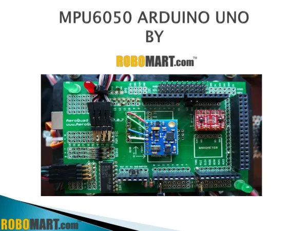
MPU6050 • MPU6050: Gyroscope + Accelerometer • ±2g, ±4g, ±8g and ±16g • ±250, ±500, ±1000, and ±2000°/sec • VCC and GND for power supply:3-5v • SCL and SDA for I2C communication with MSP430 • XCL and XDA to connect magnetic sensor Reference : MSP430 x2xx user guide MPU6050 datasheet and register file
Where to buy MSP430G2 $9.99 https://estore.ti.com/MSP-EXP430G2-MSP430-LaunchPad-Value-Line-Development-kit-P2031.aspx MPU6050 $5.75 http://www.ebay.com/itm/MPU-6050-3-Axis-Accelerometer-Sensor-Gyroscope-6DOF-Module-3-3V-5V-For-Arduino-/161108492494?pt=LH_DefaultDomain_0&hash=item2582d080ce