Download
1 / 1
10 likes | 107 Vues
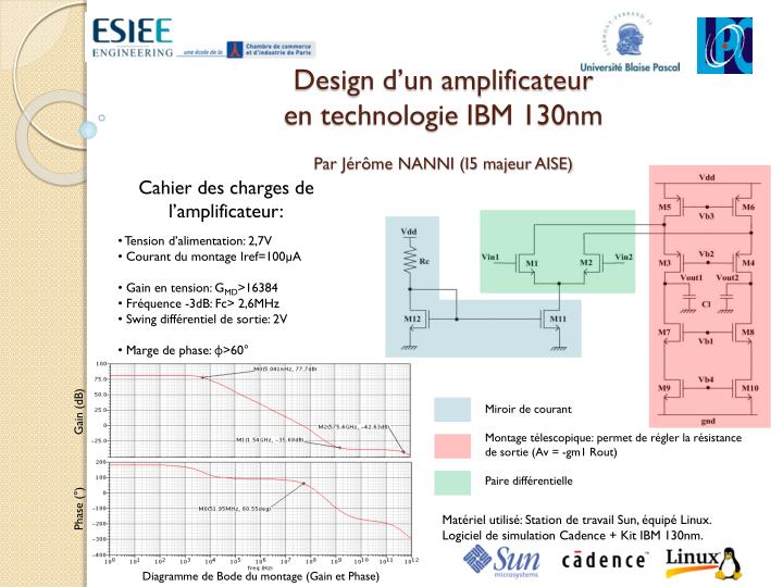
Design d’un amplificateur en technologie IBM 130nm Par Jérôme NANNI (I5 majeur AISE). Cahier des charges de l’amplificateur: Tension d’alimentation: 2,7V Courant du montage Iref =100µA Gain en tension: G MD >16384 Fréquence -3dB: Fc > 2,6MHz Swing différentiel de sortie: 2V

E N D
Design d’un amplificateur en technologie IBM 130nmPar Jérôme NANNI (I5 majeur AISE) • Cahier des charges de l’amplificateur: • Tension d’alimentation: 2,7V • Courant du montage Iref=100µA • Gain en tension: GMD>16384 • Fréquence -3dB: Fc> 2,6MHz • Swing différentiel de sortie: 2V • Marge de phase: ф>60° Phase (°) Gain (dB) Miroir de courant Montage télescopique: permet de régler la résistance de sortie (Av = -gm1 Rout) Paire différentielle Matériel utilisé: Station de travail Sun, équipé Linux. Logiciel de simulation Cadence + Kit IBM 130nm. Diagramme de Bode du montage (Gain et Phase)