Download

1 / 50
500 likes | 525 Vues
This chapter introduces sequential circuits with state tables, diagrams, latches, flip-flops, and timing characteristics. Explore various latch and flip-flop designs. Study clocked T flip-flops, PROM-based sequential circuits, and more.

E N D
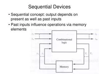
The Sequential Circuit Model Figure 6.1
State Tables and State Diagrams Figure 6.2
Sequential Circuit Example Figure 6.3
Latch and Flip-flop Timing Figure 6.4
Set Latch Figure 6.5
Reset Latch Figure 6.6
Set-Reset Latch (SR latch) Figure 6.7
NAND SR Latch Figure 6.8
Set-Reset Latch Timing Diagram Figure 6.9
SR Latch Characteristics Figure 6.11 Q* = S + RQ
SN74279 Latch with Two Set Inputs Figure 6.12
Gated SR Latch Figure 6.13
Gated SR Latch Characteristics Figure 6.14 Q* = SC + RQ + C Q
Delay Latch (D latch) Figure 6.15
D Latch Characteristics Figure 6.16 Q* = DC + CQ
D Latch Timing Diagram Figure 6.17
D Latch Timing Constraints Figure 6.18
The SN74LS75 D Latch Figure 6.19
Hazard-Free D Latch, the SN74116 Figure 6.20 Q* = DC + CQ + DC
Master-Slave SR Flip-flop Figure 6.20
SR Master-Slave Flip-Flop Characteristics Figure 6.22 Q* = S + RQ
Master-Slave D Flip-Flop Figure 6.23
Master-Slave D Flip-Flop Characteristics Figure 6.24 Q* = D
Pulse-Triggered JK Flip-Flop Characteristics Figure 6.25 Q* = KQ + JQ
Pulse-Triggered JK Flip Realization Figure 6.26
The SN7476 Dual Pulse-Triggered JK Flip-Flop Figure 6.27
SN7474 Dual Positive-Edge-Triggered D Flip-Flop Figure 6.28
SN7474 Excitation Table Figure 6.29
SN7474 Flip-Flop Timing Specifications Figure 6.30
SN74175 Positive-Edge-Triggered D Flip-Flop Figure 6.31 (a)
SN74273 Positive-Edge-Triggered D Flip-Flop Figure 6.31 (b)
SN74LS73A Edge-Triggered JK Flip-Flop Logic Diagram Figure 6.32 (a)
SN74LS73A Logic Symbols Figure 6.32 (b) and (c)
SN74276 and SN74111 Edge-Triggered JK Flip-Flops Figure 6.32 (d) and (e)
Negative-Edge-Triggered T Flip-Flop Figure 6.33
Edge-Triggered T Flip-Flop Characteristics Figure 6.34 Q* = Q
Clocked T Flip-Flop Figure 6.35
Excitation Table for Clocked T Flip-Flops Figure 6.36 Q* = TQ + TQ
The Clocked T Flip-Flop Timing Diagram Figure 6.37
SE555 Precision Timing Module Figure 6.38
Astable Operation of The SE555 Figure 6.39
Monostable (One shot) Device Realization Figure 6.40
PROM-based Sequential Circuits Figure 6.41
PROM-based Sequential Circuit Example Figure 6.41
Prime Number Sequencer Figure 6.43