Comprehensive Overview of Processor Register File Design and Control Signals
This document provides an in-depth analysis of the Register File architecture in a Processor, detailing various control signals such as write enables, multiplexer selections, and address bus interactions. It covers configurations for enabling/disabling memory operations, including the management of Data and Address Buses. Key aspects like ALU operation selection, status signals, and instruction register selections are also documented, alongside notes on signal usage in multi-input scenarios. This guide is essential for understanding the nuances of CPU design and memory interaction in educational contexts.

Comprehensive Overview of Processor Register File Design and Control Signals
E N D
Presentation Transcript
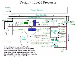
Register File + (INC) . Design 4: Edu32 Processor read=0/1 Memory System write=0/1 Data Bus (DB) Address Bus (AB) mdr_db_enb=0/1 mar_enb =0/1 pc_ab_enb=0/1 MAR ir_sel =0/1 MDR 4 mdr_sel =WB/DB 24 mar_sel=0/1 24->32 ext. PC IR mdr_enb =0/1 y_enb=0/1 pc_enb =0/1 ri_sel=0/1 16 r0_write=0/1 x_enb =0/1 rj_sel=0/1 16->32 ext. pc_sel=WB/INC rk_sel=0/1 r15_write=0/1 32 a_sel=0-15 source & dest reg addr (ri, rj, rk) b_sel=0-15 C.U. FSM Write Bus rega_sel =0/1 Status signals (m31, cout, ovfl) regb_sel =0/1 ready ALU alu_sel=ADD, ADDA, SUB, etc. op_sel =0/1 O/P Reg. Note: _sel signals to registers are used to load them; some _sel signals are more than 1 bit signals when multiple i/ps are coming into the reg. as in the PC and the MDR. This does not apply to the register file where the _sel signals have somewhat different meanings as explained in class. op_enb =0/1