Download
1 / 40
510 likes | 1.36k Vues
UNIT- V Small Signal Low Frequency Transistor Amplifier Models:.

E N D
UNIT- V Small Signal Low Frequency Transistor Amplifier Models:
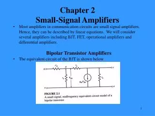
BJT: Two port network, Transistor hybrid model, determination of h- parameters, conversion of h-parameters, generalized analysis of transistor amplifier model using h-parameters, Analysis of CB, CE and CC amplifiers using exact and approximate analysis, Comparison of transistor amplifiers. • FET: Generalized analysis of small signal model, Analysis of CG, CS and CD amplifiers, comparison of FET amplifiers.
Hybrid Parameter Model Ii Io Linear Two port Device Vo Vi
h-Parameters h11 = hi = Input Resistanceh12 = hr = Reverse Transfer Voltage Ratioh21 = hf = Forward Transfer Current Ratioh22 = ho = Output Admittance
Hybrid Equivalent Model The hybrid parameters: hie, hre, hfe, hoe are developed and used to model the transistor. These parameters can be found in a specification sheet for a transistor.
Determination of parameter H22 is a conductance!
General h-Parameters for any Transistor Configuration • hi = input resistance • hr = reverse transfer voltage ratio (Vi/Vo) • hf = forward transfer current ratio (Io/Ii) • ho = output conductance
Simplified General h-Parameter Model The model can be simplified based on these approximations: hr 0 therefore hrVo = 0 and ho (high resistance on the output) Simplified
Common-Emitter re vs. h-Parameter Model • hie = re • hfe = • hoe = 1/ro
Common-Emitter h-Parameters • [Formula 7.28] • [Formula 7.29]
Common-Base re vs. h-Parameter Model • hib = re • hfb = -
Common-Base h-Parameters • [Formula 7.30] • [Formula 7.31]
SMALL-SIGNAL LOW-FREQUENCY OPERATION OF TRANSISTORS Hybrid Parameters and Two-Port Network For the hybrid equivalent model to be described, the parameters are defined at an operating point that may or may not give an actual picture of the operating condition of the amplifier. The quantities hie , hre , hfe and hoe are called the hybrid parameters and are the components of a small-signal equivalent circuit. The description of the hybrid equivalent model begins with the general two-port system. Two-port system representation (Black model realisation)
EQUIVALENT CIRCUITS THROUGH HYBRID PARAMETERS AS A TWO-PORT NETWORK For the transistor, even though it has three basic configurations, they are all four-terminal configurations, and thus, the resulting equivalent circuit will have the same format. The h-parameter will however change with each configuration. To distinguish which parameter has been used or which is available, a second subscript has been added to the h-parameter notation. (i) For the common-base configuration: the lower case letter b (ii) For the common-emitter configuration: the lower case letter e (iii) For the common-collector configuration: the lower case letter c Complete hybrid equivalent model
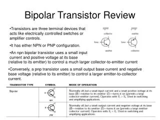
TRANSISTOR AS AMPLIFIER An n–p–n transistor in the common-base bias mode
EXPRESSIONS OF CURRENT GAIN, INPUT RESISTANCE, VOLTAGE GAIN AND OUTPUT RESISTANCE The h-parameter equivalent circuit of a transistor amplifier having a voltage source Vg , with its input resistance Rg connected to the input terminals and a load resistance RL connected to the output terminals. h-Parameter equivalent circuit of a transistor
EXPRESSIONS OF CURRENT GAIN, INPUT RESISTANCE, VOLTAGE GAIN AND OUTPUT RESISTANCE Current Gain (AI) Input Resistance (RI)
EXPRESSIONS OF CURRENT GAIN, INPUT RESISTANCE, VOLTAGE GAIN AND OUTPUT RESISTANCE Voltage Gain:- Voltage gain or voltage amplification is defined as the ratio of the output voltage V2 to the input voltage V1. Where, Output Resistance (RO)
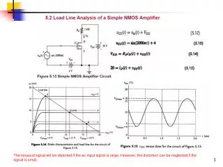
FREQUENCY RESPONSE FOR CE AMPLIFIER WITH AND WITHOUT SOURCE IMPEDANCE At different frequencies of the input signal, the performance of the device is different. The analysis till now has been limited to the mid-frequency spectrum. Frequency response of an amplifier refers to the variation of the magnitude and phase of the amplifier with frequency. a) Gain vs. frequency for a CE amplifier (b) Phase angle vs. frequency for a CE amplifier
EMITTER FOLLOWER The emitter follower transistor is a design which is basically a CC amplifier. Current gain: Input resistance: Voltage gain: Output resistance An emitter follower configuration with biasing The emitter follower is used for impedance matching.
Figure FET small-signal equivalent circuit that accounts for the dependence of iD on vDS.
For drawing an a c equivalent circuit of Amp. • Assume all Capacitors C1, C2, Cs as short circuit elements for ac signal • Short circuit the d c supply • Replace the FET by its small signal model
Analysis of CS Amplifier A C Equivalent Circuit Simplified A C Equivalent Circuit
Analysis of CS Amplifier with Potential Divider Bias This is a CS amplifier configuration therefore the input is on the gate and the output is on the drain.
Figure vo(t) and vin(t) versus time for the common-source amplifier of Figure 5.28.
An Amplifier Circuit using MOSFET(CS Amp.) Figure Common-source amplifier.
A small signal equivalent circuit of CS Amp. Figure Small-signal equivalent circuit for the common-source amplifier.
Figure vo(t) and vin(t) versus time for the common-source amplifier of Figure 5.28.
Figure Gain magnitude versus frequency for the common-source amplifier of Figure 5.28.
Figure Small-signal ac equivalent circuit for the source follower.
Figure Equivalent circuit used to find the output resistance of the source follower.