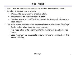
Flip-Flops
Flip-Flops. 1 0 1 0. S R Q Q’ 1 0 0 1 1 1 0 1 (after S = 1, R = 0) 0 1 1 0 1 1 1 0 (after S = 0, R = 1) 0 0 1 1. S (set) R (reset). 1 2. Q Q’ ’. (a) Logic diagram (b) Truth table. Basic RS Flip-Flop (NAND). A flip-flop holds 1 "bit".

Flip-Flops
E N D
Presentation Transcript
1 0 1 0 S R Q Q’ 1 0 0 1 1 1 0 1 (after S = 1, R = 0) 0 1 1 0 1 1 1 0 (after S = 0, R = 1) 0 0 1 1 S (set) R (reset) 1 2 Q Q’ ’ (a) Logic diagram (b) Truth table Basic RS Flip-Flop (NAND) A flip-flop holds 1 "bit". "Bit" ::= "binary digit."
D CP 3 Q Q’ 1 2 4 5 Clocked D Flip-Flop The present state is held when CP is low.
Negative Pulse Positive Pulse Positive Edge Negative Edge Negative Edge Positive Edge Clock Pulse Definition Edges can also be referred to as leading and trailing.
Y Y’ Q Q’ S R S R S R CP Master Slave MASTER-SLAVE FLIP-FLOP Master-Slave Flip-Flop
Master Slave Flip-Flop on RT54SX-A(Not hardened)
AFB BFB CFB D G ANQ BNQ CNQ B A B A B A A B C Y Y Y Y Y Y A A A A A A A B C A B C A B C A B C A B C A B C A B C Y Y Y Y Y Y S S S A Y RT54SX-S Latch(SEU Hardened)
Worst-case Military Conditions, VCCA=2.3, VCCI=3.0V, TJ=125C -1 Speed Grade Min Max Units tRCO Sequential Clock-to-Q 1.0 ns tCLR Asynchronous Clear-to-Q 0.9 ns tPRESET Asynchronous Preset-to-Q 1.0 ns tSUD Flip-Flop Data Input Set-Up 0.6 ns tHD Flip-Flop Data Input Hold 0.0 ns tWASYN Asynchronous Pulse Width 1.8 ns Flip-Flop Timing: RT54SX-S
Metastability - Introduction • Can occur if the setup, hold time, or clock pulse width of a flip-flop is not met. • A problem for asynchronous systems or events. • Can be a problem in synchronous systems. • Three possible symptoms: • Increased CLK -> Q delay. • Output a non-logic level • Output switching and then returning to its original state. • Theoretically, the amount of time a device stays in the metastable state may be infinite. • Many designers are not aware of metastability.
Metastability • In practical circuits, there is sufficient noise to move the device output of the metastable state and into one of the two legal ones. This time can not be bound. It is statistical. • Factors that affect a flip-flop's metastable "performance" include the circuit design and the process the device is fabricated on. • The resolution time is not linear with increased circuit time and the MTBF is an exponential function of the available slack time.
Metastability - Calculation • MTBF = eK2*t / ( K1 x FCLK x FDATA) t is the slack time available for settling K1 and K2 are constants that are characteristic of the flip-flop Fclock and Fdata are the frequency of the synchronizing clock and asynchronous data. • Software is available to automate the calculations with built-in tables of parameters. • Not all manufacturers provide data.
VCC Y D Q DFC1B CLR D Q DF1 EVENT SYSRESET SYSCLK CLK CLK B A AND 2A Y Synchronizer (Bad Circuit)
CLK D Q Metastable Metastable State:Possible Output from a Flip-flop
CLK Q Q Q Correct Output Metastable State:Possible Outputs from a Flip-flop Correct Output
DATA [ 3 : 0 ] CLOCK D Q DF1 D Q DF1 D Q DF1 D Q DF1 CLK CLK CLK CLK Q [ 3 : 0 ] 4-Bit Parallel Register
DATA [ 3 : 0 ] CLOCK D Q DF1 D Q DF1 D Q DF1 D Q DF1 CLK CLK CLK CLK Q [ 3 : 0 ] 4-Bit Register With Enable
Register 2 Q D Register 1 CLK Address - log2(num registers) Register Files (Simplified) D and Q are both sets of lines, with the number of lines equal to the width of each register. There are often multiple address ports, as well as additional data ports.
Decoder (AND plane) MagneticCoreMemory Register Sense wires serve as OR plane.
Data inputs Word 0 Word 1 Word 2 Word3 D0 D1 D2 D3 BC BC BC BC BC BC BC BC BC BC BC BC Address inputs Memory enable Read/write Data outputs SemiconductorMemory Decoder (AND plane) OR plane
Memory Array A5 - A11 A0 - A4 A12 - A14 CE OE VPP* Row Decoders Column Decoders Column Muxing and Sense Amps Section Select Control Logic I/O Buffers DQ0 - 7 Rad-Hard PROM Architecture No latches in this architecture
E2 Memory Array Edge Detect & Latches Row AddressDecoder Column AddressDecoder Row AddressLatches Column AddressLatches 64 Byte Page Buffer Control Latch Control Logic Timer I/O Buffer/ Data Polling W28C64 EEPROMSimplified Block Diagram A6-12 A0-5 CE* WE* Latch Enable OE* CLK VW I/O0-7 PE RSTB


