Sputtering and CVD/PVD Technology
Sputtering and CVD/PVD Technology. NANO54 Foothill College. Overview. Overview of thin film stack Fundamentals of sputtering Glow discharge, atoms in a gas state Techniques of sputtering DC and RF sputtering DC Magnetron and reactive sputtering Glow discharge CVD and PVD processes

Sputtering and CVD/PVD Technology
E N D
Presentation Transcript
Sputtering and CVD/PVD Technology NANO54 Foothill College
Overview • Overview of thin film stack • Fundamentals of sputtering • Glow discharge, atoms in a gas state • Techniques of sputtering • DC and RF sputtering • DC Magnetron and reactive sputtering • Glow discharge • CVD and PVD processes • MO-CVD, PE-CVD, plasma deposition
Thin Film Applications • Window coatings • Magnetic media • Semiconductors • Biomedical devices • Optics • Automotive • Aerospace http://spectrum.ieee.org/energy/renewables/first-solar-quest-for-the-1-watt/0
Thin Film Stack • A thin film Bragg reflector consists of a multilayer-stack of alternate high- and low-index films, all one quarter wavelength thick (see figure left). The geometrical thicknesses of the high- und low-index films are tH=l/(4nH) and tL=l/(4nL) respectively.nH and nL are the indices of refraction of the high- and low-index films, respectively and l is the center wavelength of the Bragg mirror. On every interface in the stack a part of the incident beam is reflected. The reflected parts have a phase shift of 180° only if the incident light goes from low-index medium in a high-index medium. The relative phase difference of all reflected beams is zero or a multiple of 360° and therefore they interfere constructively. The intensity of the incident light beam decreases during his travel trough the quarter-wave stack and at the same time the reflected light increases, if the absorptance ‘A’ of the stack is negligible. http://www.batop.de/information/r_Bragg.html
Thin film stack SEM image (FIB cross section SEM cross-section image of a thin film stack. Each layer is approximately 500 Angstroms thick. - http://www.jwdstaging6.com/gallery
Thin film coatings on glass (XPS, AES, TOF-SIMS, D-SIMS) XPS sputter depth profile of an architectural glass coating obtained using 2 kV argon ions and Zalar rotation to enhance depth resolution. [PHI AES] Thin films and coatings are used or applied to an almost limitless range of applications to provide a specific performance characteristic for a broad range of industrial products. These include coatings that provide antistatic properties, corrosion resistance, reduce wear, and promote adhesion; as well as thin films for optical devices, mirrors, semiconductor devices, magnetic media, and food wrap. Architectural glass, lenses, mirrors, and many other products are coated to provide specific optical properties. These coatings are often a stack of thin layers that can be characterized using PHI's surface analysis instruments to verify the composition of the layers, detect contaminants, and estimate layer thickness. http://www.phi.com/surface-analysis-applications/thin-films-and-coatings.html
Southwall XIR Film AES depth profile of Southwall Technologies XIR Film – data from Nanolab Technologies
Deposition Processes • Evaporation (thermal) • Sputter deposition (DC, RF, PE) • CVD, MO-CVD, PE-CVD • Plasma polymerized films • Solution cast (spin coating) films • Self Assembled Monolayers (SAMs)
Glow Discharge • Glow-discharge sputtering means the energetic particles used to strike target is generated by glow-discharge. Creation of glow-discharge • Tube filled with argon, neutral, no charged particles between cathode and anode • Elastic collision, no energy exchange • Inelastic collision • Energy not enough high, excite electrons, emitting photons • Energy high enough, ionize electrons, cause secondary free electrons • Both free electrons are accelerated again, so cause cascading or gas break down • Flow of electrons is collected by anode, current will quickly decay to zero
At target: target atoms ejected target ions ejected (1 - 2 %) Electrons emitted helps keep plasma going Ar+ ions reflected as Ar neutrals Ar buried in target Photons emitted Atoms into Gas State
Vacuum Deposition Physical Vapor Deposition Chemical Vapor Deposition Thermal Growth [Plasma Assisted ] Polymerization Plasma assisted Chemical growth Plasma enhanced • Evaporation [ HV, UHV, Inert Gas Reactive] • Sputtering [ HV, UHV, Inert Gas, Reactive] • Pulsed Laser Deposition [HV, UHV, Inert Gas, Reactive ]
Sputtering Process • momentum transfer process • involves top 10 Å • model as hard sphere collisions • good for energies < 50 keV • 95 % of incident energy goes into target • => COOL the target • 5 % of incident energy is carried off by target atoms • typical energies of 5-100 eV • target atoms come off with a non-uniform distribution • more atoms normal to the surface • cosine distribution (like surface source) • characterize process by sputter yield (S) • S = number ejected / number incident
S depends on: target material binding energy mass of atoms sputtering gas mass of atoms (S increases for heavier gasses) incident energy (S increases for higher energies) geometry most efficient 20-30 degrees from glancing for normal incidence sputtering: maximum around 10 kV sputtering threshold S is about 1-10 typically Sputter Yield
For calculating S we need: number of atoms ejected depends on momentum and energy transferred these depend on relative masses and collision angle maximum energy transferred to target atom in hard sphere collision depends on binding energy of target atom number of layers involved in process mean free path of ion in target typically about 2 layers surface density of target atoms collision cross section of ion with target atom Calculating S
PVD by Sputtering • Sputtering: Sputtering is a process whereby coating material is dislodged and ejected from the solid surface due to the momentum exchange associated with surface bombardment by energetic particles. Processes: • Gas ions are accelerated by a high voltage, producing a glow discharge or plasma • A source (the cathode, also called the target ) is bombarded in high vacuum by gas ions • Atoms from the target are ejected by momentum transfer and move across the vacuum chamber • Atoms are deposited on the substrate to be coated and form a thin film.
Sputtering Mechanism The kinetic energy of the impinging particles largely dictates what event will happen • Bounce back : when very low energy (<5eV); when the collision is head-on or nearly so • Embedded : when much higher energy (>10KeV), the impinging particles are most likely to be embedded in the target, which is the basis of Ion Implantation • If energy level is between the two extremes: • some fraction of the energy of the impinging ions is transferred to the solid in the form of heat, and lattice damage • another fraction of such energy causes atoms from the surface to be dislodged and ejected into the gas phase----Sputtering
Unique Characteristics • Uniform thickness over large area. • Simple thickness control. • The alloy composition maintains stoichiometry with the original target composition. • Deposition rates do not differ a great deal from one material to another. • Sputtering-cleaning prior to initiating film deposition. The surface is not again exposed to ambient after such cleaning. • The lifetime of a sputtering target may be as long as hundreds of runs and is seldom less than 20.
Coating Materials Metals: Al, Cu, Zn, Au, Ni, Cr, W, Mo, Ti Alloys Ag-Cu, Pb-Sn, Al-Zn, Ni-Cr Nonmetals:graphite, MoS2, WS2, PTFE Refractory oxides:Al2O3, Cr2O3, Al2O3-Cr2O3, SiO2, ZrO2-Y2O3 Refractory carbides:TiC, ZrC, HfC, NbC, Tic-Ni, Tic-ZrC Refactory nitrides:TiN, Ti2N, ZrN, HfN, TiN-ZrN, TiN-AlN-ZrN Refractory borides:TiB2, ZrB2, HfB2, CrB2, MoB2 Refactory silicides:MoSi2, WSi2, Cr3Si2
DC Sputter Deposition Sputter deposition is a physical vapor deposition (PVD) method of depositingthin films by sputtering, that is ejecting, material from a "target," source, which then deposits onto a "substrate," such as a silicon wafer. Sputtered atoms ejected from the target have a wide energy distribution, typically up to tens of eV (100,000 K). The sputtered ions (typically only a small fraction (~1% of the ejected particles are ionized) can ballistically fly from the target in straight lines and impact energetically on the substrates or vacuum chamber (causing resputtering). Energetic ions sputter material off the target which diffuse through the plasma towards the substrate where it is deposited. There is no strong plasma glow around the cathode since it takes a certain distance for the plasma to be generated by electron avalanches started by a few secondary electrons from the sputtering process. http://en.wikibooks.org/wiki/Microtechnology/Additive_Processes
Sputtering alloy targets composition of alloy in film is approximately the same as alloy in target (unlike evaporation) rapid mixing in liquids (evaporation) slow diffusion mixing in solids (sputtering) target reaches steady state surface composition balances sputter yield Process: Initial alloy of A and B .......................... ABABABABABABAB If SA > SB , remove more A enriches surface in B .................... . BAB. B. BA. B . AB More B on surface => more B sputtered ....... ABABBABABBAB surface composition reaches steady state surface enriched in B bulk composition sputtered fASA / CA = fBSB / CB where f = surface fraction and C = bulk composition alloy targets need to be conditioned by sputtering a few hundred Å before depositing
2. Transport to substrate Target atoms pass through Ar gas and plasma environment one Ar+ ion for every 10,000 Ar neutrals electrons in plasma collide with Ar neutrals to form ions and more electrons Target atoms collide with Ar atoms, Ar+ ions and electrons treat as random walk "diffusion" through gas target atoms lose energy (down to 1-10 eV) chemical reactions may occur in gas not a line of sight process (unless pressure reduced) can coat around corners
3. Deposit on substrate target atoms and ions impinge electrons impinge Ar atoms impinge Ar pressure about 0.1 torr Ar may be incorporated into film energetic particles may modify growth substrates heat up 100 - 200 C is common for a thermally isolated sample (no heat conduction) r = substrate density (g/cm3) c = substrate heat capacity (J/gûC) d = substrate thickness (cm) W = film atomic volume (cm3/atom) D-DOT = deposition rate (Å/min) t = time (secs) energies are in eV/atom note: the constant does have units
optimum deposition rate around 100 mTorr compromise between increasing number of Ar ions increasing scattering of Ar ions with neutral Ar atoms if you can increase the number of ions without increasing the number of neutrals, you can operate at lower pressures Sputter voltage maximize sputter yield (S) typically -2 to -5 kV Substrate Bias Voltage substrate is being bombarded by electrons and ions from target and plasma sputtering film while you deposit neutral atoms deposit independently put negative bias on the substrate to control this can significantly change film properties Substrate temperature control with substrate heater heating from deposited material increases with increasing sputter voltage decreases with increasing substrate bias Deposition rate changes with Ar pressure increases with sputter yield usually increases with high voltage Particle Energy increases with increasing sputter voltage decreases with increasing substrate bias decreases with increasing Ar pressure
Good for insulating materials in DC systems, positive charge builds up on the cathode (target) need 1012 volts to sputter insulators !! avoid charge build up by alternating potential • . . . . . . . . . . . . . . . . TIME -------> • sputter deposition occurs when target is negative • substrate and chamber make a very large electrode - so not much sputtering of substrate • Physical process • frequencies less than about 50 kHz • electrons and ions in plasma are mobile • both follow the switching of the anode and cathode • basically DC sputtering of both surfaces • frequencies above about 50 kHz • ions (heavy) can no longer follow the switching • electrons can neutralize positive charge build up
Advantages: Easier to keep plasma going under these conditions Can operate at lower Ar pressures (1-15 mTorr) fewer gas collisions => more line of sight deposition
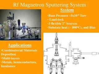
Magnetron Sputter Deposition • use with DC or RF • goal: increase ionization of Ar • Why? Higher sputter rates at lower Ar pressures (down to 0.5 mTorr) • fewer gas collisions - more line of sight • How ? increase probability of electrons striking Ar • increase electron path length • use electric and magnetic fields • Most common configuration: crossed electric and magnetic fields • Put magnets (200 Gauss) behind target: • traps electrons near cathode • more ionization near cathodes (10x) • fewer electrons reach substrate (less heating)
Ion Assisted Deposition • with evaporation or sputtering (or chemical vapor deposition) • bombard surface with ions • not necessarily same type as in film • ions typically NOT incorporated in film • relatively low voltages (50 - 300 eV) • leads to • physical rearrangement • local heating • can change film properties • for better or worse • disruption of columnar growth requires about 20 eV of added energy per depositing atom
Reactive Sputter Deposition • Add reactive gas to chamber during deposition (evaporation or sputtering) • oxygen, nitrogen • Chemical reaction takes place on substrate and target • Can poison target if chemical reactions are faster than sputter rate • Adjust reactive gas flow to get good stoichiometry without incorporating excess gas into film