Sputtering
Sputtering. Eyal Ginsburg. WW49/00 . Contents. Metallization structure Uses for different layers Step Coverage Sputtering: yield, conditioning, methods. Metallization Structure.


Sputtering
E N D
Presentation Transcript
Sputtering Eyal Ginsburg WW49/00
Contents • Metallization structure • Uses for different layers • Step Coverage • Sputtering: yield, conditioning, methods
Metallization Structure • The semiconductor industry uses PVD to deposit the metal that electrically connects the various parts of the IC to each other and to the outside world. • There are four common structure in metallization: contacts, vias, plugs and interconnects. • Contact: A hole in the Si dioxide layer that connect the transistors to the first metal layer.
Metallization Structure (Cont.) • Via: A hole in the Si dioxide layer that connect two metal layers. • Plug: A metal layer that fills either a contact or a via. Made of either tungsten (W) or aluminum (Al). • Interconnect: Metal layer. The IC has more than one layer of interconnects, each layer has different name, starting with the first layer deposited, “Metal 1”, “Metal 2”, etc.
Contact / Via / Plug / Interconnect Via 2 Interconnects Metal 3 Silicon Dioxide (ILD) Metal 2 Silicon Dioxide (ILD) Via 1 Metal 1 Contact Silicon Dioxide Silicon
Glue Layer or Adhesion layer • Companies commonly use the WCVD process to fill contacts/vias with tungsten. Unfortunately, if one uses WCVD to deposit W directly to SiO2, the W flakes and peels, producing many particles. • Therefore, an intermediate layer is deposited between the oxide and WCVD.
W TiN Ti Glue Layer (Cont. 1) • The most common process: • Deposit Ti layer onto silicon oxide • Deposit TiN onto Ti • Deposit WCVD
W filled Contact/Via • Ti reduce contact resistance • Reacts with Si to form Silicide. • Acts as Getter to reduce native oxide resistance (Ti reacts with oxygen at the bottom of the hole). • TiN prevents W from peeling • Stop WF6 from reacting with Ti or SiO2. • Called glue or adhesion layer. • W carries current from Si to interconnect and called “plug”.
Aluminum - General • Al-alloys thin films were selected for the first 30 years of the IC industry. • They continue to be the most widely used materials, although copper. • Al has low resistivity (=2.7-cm), and its compatibility with Si and SiO2. • Al forms a thin native oxide (Al2O3) on its surface upon exposure to oxygen, and affect the contact resistance.
Aluminum - General (cont. 1) • Al thin films can also suffer from corrosion (ex. Al dry etch may leave chlorine residues on Al surface and lead to formation of HCl and then attack the Al).
Aluminum interconnects • The material used in interconnects is not pure aluminum, but an aluminum alloy. Usually with Cu (0.5-2%), sometimes with Si. • The Cu in Al-alloy slows the electromigration (EM) phenomenon. Si slows EM slightly, used in contact level to prevent spiking. • Al-alloys decrease the melting point, increase the resistivity and need to be characterized (ex. Dry etch).
Aluminum contact • Aluminum can be used to fill contacts. Unfortunately, with Al you encounter a problem that don’t finds with WCVD: Si dissolves into Al at high temp (>450ºC) which cause a failure called “spiking”.
Al contact (Cont. 1) • To prevent it • We placed a barrier layer : TiN or TiW. • And by using Al-Si alloy (which essentially predissolving Si into the Al).
Al Ti TiN SiO2 Aluminum contact – process flow • 1st Ti layer reduces contact resistance • TiN layer stops Si from from diffusing into Al (Barrier layer) • 2nd Ti layer helps Al form continues film (wetting layer) • Al fills contact and forms interconnect
Aluminum Via • If you fill a via with Al, spiking is not a problem, since the Al dose not come into contact with any Si. • Barrier layers are not necessary. • Most applications do still use a layer of Ti, because Al forms a much smoother film on top of Ti than on SiO2 (Wetting layer). • Al fills Via and forms interconnect.
ARC Layer • In the photolithography step that follows aluminum, the high reflectivity of Al can present large problem. The light can pass through the PR, reflect off of the Al and expose areas of PR that should not be exposed.
ARC Layer (Cont. 1) • Therefore we deposit a layer that stops the light from reflecting off of the Al. • The layer is called an “Anti Reflective Coating” layer or ARC layer. • Common PVD layers are TiN or TiW. • TiN has a very low reflectivity at a 436nm wavelength, this is the same wavelength that the resist is exposed to during photolithography.
TiN for Hillock Suppressant • Hillock Suppressant is the second purpose for the TiN Arc layers. • Hillocks are a result of stress relief between the underlying dielectric and the metal layers. This stress arises from the different thermal expansion coefficients and can cause protrusions (hillocks) of the dielectric into the metal. • This is undesirable since the metal is thinner, it is more susceptible to EM. • TiN has a compressive film stress, it aids in suppressing the hillocks.
Metal line – stack Usually the metal line contains 4-5 layers: • Al - This layer makes the contacts with the Tungsten plugs. It is the primary current carrier. • TiN Layer - Creates a barrier between the Al/Cu and the Titanium layers because of the increasing temperature at a downstream process will increase the rate of the reaction of Al with Ti.
Metal stack (Cont. 1) • Titanium Layer - Provides an alternate current path (shunt) around flaws in the primary current carrier. And thus improves electromigration characteristics.
Metal stack (Cont. 2) • TiN ARC Layer - This is an anti‑reflecting coating which aides lithography to keep control of critical dimensions and to absorb light during the resist exposure. It also functions as a hillock suppressant.
Last metal line • The Titanium layers is deposited first because the last metal layer must connect to the bond pads that connect the microprocessors to the outside world. The bond pads adhere poorly to Titanium, but they adhere well to Al/Cu. • The Al/Cu is deposited second. • There is no TiN buffer layer between Titanium and Al/Cu layers because there are no high temperature steps.
tc to H tb D After deposition Before deposition What is step coverage ? • It is a measure of how well the film covers topography. Definitions: to = field thk tb/to = bottom coverage Tb = bottom thk tc = cusping thk H/D = Aspect Ratio (A/R)
Step coverage issues • The Aspect Ratio dependence of step coverage is critical into the submicron regime. • Cusping can lead to voids. • Voids in metal films can cause problems: • Increased resistance. • Trap impurities. • Non-repeatable results. • Decrease the cross sectional area that increase electromigration (high current density).
PVD Vs. CVD PVD • Metal is transported from target to substrate. • Deposition is “line of sight”. • Poor step coverage (can be improved by increasing the surface-migration ability by raising the substrate temperature). CVD • Chemical reaction. • Excellent step coverage.
Step coverage trends • Cause: • Devices are getting smaller. • Aspect Ratio are getting higher. • Then: • Planarization process bring vias with same depth. • Contact to Metal 2 was allowed only through Metal 1. • Vias with sloped sidewalls but have a conflict with design rules. • Sputter CVD Electroplating
SEM interconnects • Example of contact to Metal 2 was allowed only through Metal 1. • Dielectric layers etched away
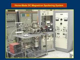
Sputtering – General • Sputtering is a term used to describe the mechanism in which atoms are ejected from the surface of a material when that surface is stuck by sufficiency energetic particles. • Alternative to evaporation. • First discovered in 1852, and developed as a thin film deposition technique by Langmuir in 1920. • Metallic films: Al-alloys, Ti, TiW, TiN, Tantalum and Cobalt.
Reasons for sputtering • Use large-area-targets which gives uniform thickness over the wafer. • Control the thickness by Dep. time and other parameters. • Control film properties such as step coverage (negative bias), grain structure (wafer temp), etc. • Sputter-cleaned the surface in vacuum prior to deposition.
Sputtering steps • Ions are generated and directed at a target. • The ions sputter targets atoms. • The ejected atoms are transported to the substrate. • Atoms condense and form a thin film.
The billiard ball model • There is a probability that atom C will be ejected from the surface as a result of the surface being stuck by atom A. • In oblique angle (45º-90º) there is higher probability for sputtering, which occur closer to the surface.
Sputter yield • Defined as the number of atoms ejected per incident ion. • Typically, range 0.1-3. • Determines the deposition rate. • Depends on: • Target material. • Mass of bombarding ions. • Energy of the bombarding ions. • Direction of incidence of ions (angle).
Sputter yield (Cont. 1) • Sputter yield peaks at <90º. • Atoms leave the surface with cosine distribution.
Process conditions • Type of sputtering gas. In purely physical sputtering (as opposed to reactive sputtering) this limits to noble gas, thus Argon is generally the choice. • Pressure range: usually 2-3 mTorr (by glow discharge). • Electrical conditions: selected to give a max sputter yield (Dep rate).
Sputter deposition film growth • Sputtered atoms have velocities of 3-6E5 cm/sec and energy of 10-40 eV. • Desire: many of these atoms deposited upon the substrate. • Therefore, the spacing is 5-10 cm. • The mean free path is usually <5-10 cm. • Thus, sputtered atoms will suffer one or more collision with the sputter gas.
Sputter dep. film … (Cont. 1) • The sputter atoms may therefore: • Arrive at surface with reduce energy (1-2 eV). • Be backscattered to target/chamber. • The sputtering gas pressure can impact on film deposition parameters, such as Dep rate and composition of the film.
Sputtering - methods • Reactive sputtering • RF sputtering • Bias sputtering • Magnetron sputtering • Collimated sputtering • Hot sputtering
Reactive sputtering • Reactive gas is introduced into the sputtering chamber in addition to the Argon plasma. • The compound is formed by the elements of that gas combining with the sputter material (Ex. TiN). • The reaction is usually occurs either on the wafer surface or on the target itself.
Reactive sput. (Cont. 1) • In case of TiN, the Nitrogen reacts with the Ti on the surface of the target, and then it is sputtered onto the wafer.
RF sputtering • DC sputter deposition is not suitable for insulator deposition. • RF voltages can be coupled capacitively through the insulating target to the plasma, so conducting electrodes are not necessary. • The RF frequency is high enough to maintain the plasma discharge.