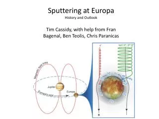
Sputtering
Sputtering. Eyal Ginsburg. WW46/02 . Contents. Metallization structure PVD System Overview Sputtering: yield, conditioning, methods Film nucleation and growth. W Plug Via 2. M3. M2. M1. Silicon substrate. Contact & Metal Lines - SEM. Glue Layer (Cont. 1). Aluminum - General.


Sputtering
E N D
Presentation Transcript
Sputtering Eyal Ginsburg WW46/02
Contents • Metallization structure • PVD System Overview • Sputtering: yield, conditioning, methods • Film nucleation and growth
W Plug Via 2 M3 M2 M1 Silicon substrate Contact & Metal Lines - SEM
Aluminum - General • Al-alloys thin films were selected for the first 30 years of the IC industry. • They continue to be the most widely used materials, although copper. • Al has low resistivity (=2.7-cm), and its compatibility with Si and SiO2. • Al forms a thin native oxide (Al2O3) on its surface upon exposure to oxygen, and affect the contact resistance.
Aluminum - General (cont.) • Al thin films can also suffer from corrosion (ex. Al dry etch may leave chlorine residues on Al surface and lead to formation of HCl and then attack the Al).
Aluminum interconnects • The material used in interconnects is not pure aluminum, but an aluminum alloy. Usually with Cu (0.5-2%), sometimes with Si. • The Cu in Al-alloy slows the electromigration (EM) phenomenon. Si slows EM slightly, used in contact level to prevent spiking. • Al-alloys decrease the melting point, increase the resistivity and need to be characterized (ex. Dry etch).
Metal line – stack Usually the metal line contains 4-5 layers: • Al - This layer makes the contacts with the Tungsten plugs. It is the primary current carrier. • TiN Layer - Creates a barrier between the Al/Cu and the Titanium layers because of the increasing temperature at a downstream process will increase the rate of the reaction of Al with Ti.
Metal stack (Cont. 1) • Titanium Layer - Provides an alternate current path (shunt) around flaws in the primary current carrier. And thus improves electromigration characteristics.
Metal stack (Cont. 2) • TiN ARC Layer - This is an anti‑reflecting coating which aides lithography to keep control of critical dimensions and to absorb light during the resist exposure. It also functions as a hillock suppressant.
Metal stack - SEM Metal line ILD TiN W- Via2 Ti TiN Metal line Al
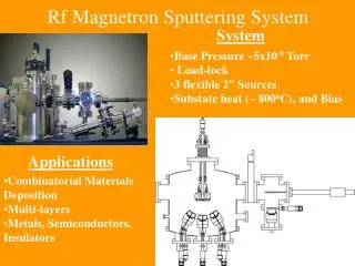
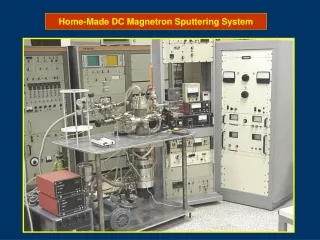
Mainframe Components • Preclean Ch. – Applies a light. Non selective plasma etch to the wafer before the PVD process. • Cooldown Ch. – Cools the wafer after the PVD process. • Expansion Ch. (C&D) – Optionally configured for PVD or other processes such as etch. • Wafer orienter/degas Ch. – Orients the wafer flat to a designated angle and degasses the wafer to remove water vapor before the preclean process. • PVD Ch. – DC magnetron sputter deposition chambers for depositing materials used in interconnects metalization (ex. Al, Ti, TiN, TiW). • Cassette loadlocks – The starting point for wafer transfers. Accept 1 cassette with 25 wafers.
Vacuum system • PVD system uses Ultra-High Vacuum (UHV) to reduce particulates and provide purer film qualities. • The tool uses staged vacuum regimes to achieve UHV.
Sputtering – General • Sputtering is a term used to describe the mechanism in which atoms are ejected from the surface of a material when that surface is stuck by sufficiency energetic particles. • Alternative to evaporation. • First discovered in 1852, and developed as a thin film deposition technique by Langmuir in 1920. • Metallic films: Al-alloys, Ti, TiW, TiN, Tantalum, Nickel, Cobalt, Gold, etc.
Reasons for sputtering • Use large-area-targets which gives uniform thickness over the wafer. • Control the thickness by Dep. time and other parameters. • Control film properties such as step coverage (negative bias), grain structure (wafer temp), etc. • Sputter-cleaned the surface in vacuum prior to deposition.
Sputtering steps • Ions are generated and directed at a target. • The ions sputter targets atoms. • The ejected atoms are transported to the substrate. • Atoms condense and form a thin film.
Sputtering Coating process that involves the transport of material from the target to the wafer. Atoms from the target are ejected as a result of momentum transfer between incident ions and the target. The particles traverse the vacuum chamber and are deposited on the wafer.
Application of Sputtering • Thin film deposition: • Microelectronics • Decorative coating • Protective coating • Etching of targets: • Microelectronics patterning • Depth profiling microanalysis • Surface treatment: • Hardening • Corrosion treatment
The billiard ball model • There is a probability that atom C will be ejected from the surface as a result of the surface being stuck by atom A. • In oblique angle (45º-90º) there is higher probability for sputtering, which occur closer to the surface.
Sputter yield • Defined as the number of atoms ejected per incident ion. • Typically, range 0.1-3. • Determines the deposition rate. • Depends on: • Target material. • Mass of bombarding ions. • Energy of the bombarding ions. • Direction of incidence of ions (angle). • Pressure
Sputter yield (Cont. 1) Target materials: Al/Cu(0.5%) 2 Grain size: 200m 1 Grain size: 45m
Sputter yield (Cont. 2) • Molecule size – need to be about the same size as the sputtered material: • too big cause layer deformation and yield a lot of material. • too small cause layer deformation w/o ejecting atoms. Target deformation = Less uniform dep.
Sputter yield (Cont. 3) Ion energy Vs. sputter yield:
Sputter yield (Cont. 4) • Sputter yield peaks at <90º. • Atoms leave the surface with cosine distribution.
Sputter yield (Cont. 5) • Pressure reduction – allow better deposited atoms/molecules flux flow towards the substrate. Expressed by “Mean free path” which is the average distance an atom can move, in one direction without colliding at another atom.
Process conditions • Type of sputtering gas. In purely physical sputtering (as opposed to reactive sputtering) this limits to noble gas, thus Argon is generally the choice. • Pressure range: usually 2-3 mTorr (by glow discharge). • Electrical conditions: selected to give a max sputter yield (Dep rate).
Sputter deposition film growth • Sputtered atoms have velocities of 3-6E5 cm/sec and energy of 10-40 eV. • Desire: many of these atoms deposited upon the substrate. • Therefore, the spacing is 5-10 mm. • The mean free path is usually <5-10 mm. • Thus, sputtered atoms will suffer one or more collision with the sputter gas.
Sputter dep. film … (Cont. 1) • The sputter atoms may therefore: • Arrive at surface with reduce energy (1-2 eV). • Be backscattered to target/chamber. • The sputtering gas pressure can impact on film deposition parameters, such as Dep rate and composition of the film.
Sputtering – additional methods • Reactive sputtering • RF sputtering • Magnetron sputtering • Collimated sputtering • Hot sputtering
Reactive sputtering • Reactive gas is introduced into the sputtering chamber in addition to the Argon plasma. • The compound is formed by the elements of that gas combining with the sputter material (Ex. TiN). • The reaction is usually occurs either on the wafer surface or on the target itself. • As you add more reactive gas at some point the reaction rate exceeds the sputtering rate. • At this point the target surface switches from clean metal to compound over a short time.
Reactive sput. (Cont. 1) • The transition in target chemistry changes sputtering conditions dramatically !
Reactive sput. (Cont. 2) Typical compounds deposited by reactive sputtering:
RF sputtering • DC sputter deposition is not suitable for insulator deposition, because the positive charge on the target surface rejects the ion flux and stop the sputtering process. • RF voltages can be coupled capacitively through the insulating target to the plasma, so conducting electrodes are not necessary. • The RF frequency is high enough to maintain the plasma discharge.
RF sputtering (Cont. 1) • During the first few complete cycles more electrons than ions are collected at each electrode (high mobility), and cause to negative charge to be buildup on the electrodes. • Thus, both electrodes maintain a steady-state DC potential that is negative with respect to plasma voltage, Vp. • A positive Vp aids the transport of the slower positive ions and slow down the negative electrodes.
RF sputtering (Cont. 2) • The induced negative biasing of the target due to RF powering means that continuous sputtering of the target occurs throughout the RF cycle. • But it is also means that this occurs at both electrodes.
RF sputtering (Cont. 3) • The wafer will be sputtered at the same rate as the target since the voltage drops would be the same at both electrodes for symmetric system. • It would thus be very difficult to deposit any material in that way. • Smaller electrode requires a higher RF current density to maintain the same total current as the larger electrode.
RF sputtering (Cont. 4) • By making the area of the target electrode smaller than the other electrode, the voltage drop at the target electrode will be much greater than at the other electrode. • Therefore almost all the sputtering will occur at the target electrode.
RF sputtering (Cont. 5) • We also use RF sputtering to clean out bottoms of Contacts and Vias before the actual deposition. • Remove native oxides and etch residues from Contacts/Vias. • During this step, a controlled thickness of surface material is sputtered off the wafer, removing any contaminants or native oxide. • A film can then be sputter deposited immediately afterward without breaking the vacuum. • This process was done in the pre-clean chamber. • This may also be done by BIAS SPUTTERING (reversing the electrical connections).
Magnetron sputtering • Here magnets are used to increase the percentage of electrons that take part in ionization events, increase probability of electrons striking Ar, increase electron path length, so the ionization efficiency is increased significantly. • Another reasons to use magnets: • Lower voltage needed to strike plasma. • Controls uniformity. • Reduce wafer heating from electron bombardment. • Increased deposition rate
Magnetron sputtering (Cont. 1) • Lower voltage: • Magnets produce magnetic field • Magnetic field make an electron go in curved path (helix) • Curved paths are longer more collisions • More collisions make more ions easier to strike plasma. • Controls uniformity: • Electrons paths are more curved near stronger magnetic field. • More ions collide with target in regions of high magnetic field. • More ion collisions lead to more target atoms sputtering. • More magnets near edge/center makes edge/center thick deposition.
Magnetron sputtering (Cont. 2) • A magnetic field is applied at right angle to electric field by placing large magnets behind the target. • This traps the electrons near the target surface, and causes them to move in spiral motion until the collide with an Ar atom. • Dep rate increases up to 10-100 times faster than without magnetron configuration.
Magnetron sput (Cont. 3) • Magnetron sputtering can be done in either DC or RF modes, but the former is more common. • Target erodes rapidly in the ring region resulting in a deep groove in the target face, which cause to non-uniformity film.
Collimated sputtering • During the PVD process, metal atoms are sputtered at all angles. The standard process deposits metal on all areas of the process kit and at various angles on the wafer. • A small range of arrival angles during deposition can cause nonuniform film. • This leads to poor bottom coverage of small geometry, high aspect ratio contacts and vias as the “holes” seal off at the top before filling up at the bottom.
Collimated sput. (Cont. 1) • One way to improve this by having a narrow range of arrival angles, while atoms arriving perpendicularly to the wafer. • This method called collimated sputtering (first proposed in 1992). • A hexagonal holes plate is placed between the target and the wafer.