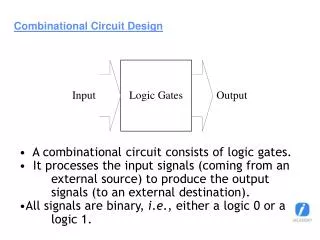
Combinational Circuit Description Modified from ECE574 Notes by Prof. Navabi
Combinational Circuit Description Modified from ECE574 Notes by Prof. Navabi. Combinational Circuit Description. 4.1 Module Wires 4.1.1 Ports 4.1.2 Interconnections 4.1.3 Wire values and timing 4.1.4 A simple testbench 4.2 Gate Level Logic 4.2.1 Gate primitives

Combinational Circuit Description Modified from ECE574 Notes by Prof. Navabi
E N D
Presentation Transcript
Combinational Circuit Description Modified from ECE574 Notes by Prof. Navabi
Combinational Circuit Description 4.1 Module Wires 4.1.1 Ports 4.1.2 Interconnections 4.1.3 Wire values and timing 4.1.4 A simple testbench 4.2 Gate Level Logic 4.2.1 Gate primitives 4.2.2 User defined primitives 4.2.3 Delay formats 4.2.4 Module parameters
Combinational Circuit Description 4.3 Hierarchical Structures 4.3.1 Simple hierarchies 4.3.2 Vector declarations 4.3.3 Iterative structures 4.3.4 Module path delay 4.4 Describing Expressions with Assign Statements 4.4.1 Bitwise operators 4.4.2 Concatenation operators 4.4.3 Vector operations 4.4.4 Conditional operation 4.4.5 Arithmetic expressions in assignments 4.4.6 Functions in expressions 4.4.7 Bus structures 4.4.8 Net declaration assignment
Combinational Circuit Description 4.5 Behavioral Combinational Descriptions 4.5.1 Simple procedural blocks 4.5.2 Timing control 4.5.3 Intra-assignment delay 4.5.4 Blocking and nonblocking assignments 4.5.5 Procedural if-else 4.5.6 Procedural case statement 4.5.7 Procedural for statement 4.5.8 Procedural while loop 4.5.9 A multilevel description
Combinational Circuit Description 4.6 Combinational Synthesis 4.6.1 Gate level synthesis 4.6.2 Synthesizing continuous assignments 4.6.3 Behavioral synthesis 4.6.4 Mixed synthesis 4.7 Summary
Module Wires • Wires or nets are used for interconnection of substructures together, and interconnection of module ports to appropriate ports of a module’s substructures. • By default module ports are wires (net). • Wires have delays, can take ant of the four values (0, 1, Z and X).
Ports Ports
Ports • Ports are allowed to be defined as input, output or inout. • Aninputport is always a net and can only be read. • An output is a net by default, and can be declared as a reg if it is to be assigned a value inside a procedural block. • Aninout is a bidirectional port that can be written into or read from. An inout port is always a net.
Ports Ports `timescale 1ns/100ps module Anding (input a, b, output y); and (y, a, b); endmodule • A Simple Module
Ports The symbol of input ports The symbol of output ports • Multiplexer using Tri-state buffers
Interconnections The and primitive generates its output, which is carried through the y net to the output of Anding. `timescale 1ns/100ps module Anding (input a, b, output y); and (y, a, b); endmodule Values put into the a and b inputs of Anding are carried through these wires to the inputs of and. • A Simple Module
Wire Values and Timing Wire Values and Timing
Wire Values and Timing • A net used for a module port or an internal interconnection can take any of the four Verilog logic values, i.e., 0, 1, Z, and X. • Such a value assigned to a net can have a delay, which may be specified by the assignment to the net or as part of its declaration. • Multiple simultaneous assignments to a net, or driving a net by multiple sources is legal and the result is defined by the type of the net.
Wire Values and Timing Multiplexer built by tri-state buffers Tri-state buffers • Multiplexer using Tri-state buffers
Wire Values and Timing `timescale 1ns/100ps module TriMux (input i0, i1, sel, output y); wire sel_ ; not #5 g0 (sel_, sel); bufif1 #4 g1 (y, i0, sel_), g2 (y, i1, sel ); endmodule Instance Name Optional for primitive instantiations A Delay of 5ns for the not gate Two instances of bufif1 are combined into one gate instantiation construct • Verilog for a Multiplexer with Tri-state Buffers
Wire Values and Timing • Simulation Results of buff1 At time 34 ns, both g1 and g2 conduct. g1 is still conducting because it takes the not gate 5 ns to change the value of sel_ and bufif1 an extra 4 ns to stop g1 from conducting. This causes the value X to appear on y. At time 45 ns sel becomes 0. Because of this change, after a 4ns delay, neither g1 nor g2 conduct, causing a Z (high impedance) to appear on y for a period of 5 ns (inverter delay). • Simulation Results of bufif1 Because of the delay of the not gate, this X value remains on y for 5 ns.
A Simple Testbench A Simple Testbench
A Simple Testbench Because i0, i1, and s must be assigned values in this testbench, they are declared as reg and initialized to 0. `timescale 1ns/100ps module TriMuxTest; reg i0=0, i1=0, s=0; wire y; TriMux MUT (i0, i1, s, y); initialbegin #15 i1=1’b1; #15 s=1’b1; #15 s=1’b0; #15 i0=1’b1; #15 i0=1’b0; #15 $finish; end endmodule The initial statement is a procedural construct and uses delay control statements to delay the program flow in this procedural block. The delay before $finish allows the last input change to have a chance to affect the circuit output. • A Testbench for TriMux
Gate Primitives Gate Primitives
Gate Primitives • Basic Gate Primitives
Gate Primitives • Gates categorized as n_input gates are and, nand, or, nor, xor, and xnor. • An n_input gate has one output, which is its left-most argument, and can have any number of inputs. nand #(3, 5) gate1 (w, i1, i2, i3, i4); A 4-input nand tPLH (low to high propagation) and tPHL (high to low propagation) times are 3 and 5, respectively.
Gate Primitives A majority circuit (maj3) with a, b, c input and y output. For connecting and gate outputs to the output or gate, intermediate wires im1, im2, and im3 are used. • Majority Circuit
Gate Primitives `timescale 1ns/100ps module maj3 (a, b, c, y); input a, b, c; output y; wire im1, im2, im3; and #(2, 4) ( im1, a, b ), ( im2, b, c ), ( im3, c, a ); or #(3, 5) (y, im1, im2, im3); endmodule The and primitive name and its delay specification are shared between the three instances of this gate. The or gate uses 3 and 5 ns for its delay parameters and drives the y output of the circuit. • Majority Verilog Code
User Defined Primitives User Defined Primitives
User Defined Primitives • Verilog primitives: simple functions, more complex functions can be formed based on them. • For simple functions for which Verilog does not provide a primitive, a user-defined primitive (UDP) can be formed. • A combinational UDP can form a combinational function of up to 10 inputs and one output. • The definition of a UDP can only include a table in the form of a logical Truth Table. • A UDP output can only be specified as a 0 or a 1. The Z value cannot be specified, and an X happens for unspecified input combinations. • A UDP definition cannot include delay values, but when instantiating it, rise and fall (tPLH and tPHL) delay values can be specified. • The initial value of the output of a UDP is X, which changes to a 0 or a 1 after the specified delays.
User Defined Primitives A UDP definition begins with primitive keyword The output of a UDP is always first in its port list. primitive maj3 (y, a, b, c); output y; input a, b, c; table 0 0 ? : 0; 0 ? 0 : 0; ? 0 0 : 0; 1 1 ? : 1; 1 ? 1 : 1; ? 1 1 : 1; endtable endprimitive In the table, a ? stands for a 0, 1 and an X. Therefore, 00? expands to 000, 001, and 00X. For all of them maj3 produces the same output. • Majority UDP
Delay Formats Delay Formats
Delay Formats • A two-value gate such as an and and an xor uses a delay2 construct for its delay specification. • For a tri-state gate a delay3 language construct is used that specifies its delay to 1, to 0, and to Z. • For these gates, zero, one, two, or three delay values may be specified. • In the absence of the third value, minimum of the first two will be used for transitions to Z. Likely, transitions to X always take the minimum of the specified values. • Instead of a fixed delay value, min:typ:max delay may be used: • Specifies the minimum, typical, and maximum delay values. • Called a delay expression and by default typ is used in simulation. • Overriding this default and using the other specified values can be done by a simulation switch.
Delay Formats • Three-input XOR
Delay Formats module xor3_mtm (input a, b, c, output y); wire a_, b_, c_; wire im1, im2, im3, im4; not #(1:3:5, 2:4:6) ( a_, a ), ( b_, b ), ( c_, c ); nand #(2:4:6, 3:5:7) ( im1, a_, b_, c ), ( im2, a_, b, c_ ), ( im3, a, b_, c_ ), ( im4, a, b, c ); nand #(2:4:6, 3:5:7) (y, im1, im2, im3, im4); endmodule By default, simulation will be done with typ delay values, i.e., 3 and 4 for not and 4 and 5 for nand gates • Verilog Code Using min:typ:max Delay
Module Parameters Module Parameters
Module Parameters • Parameters can be used for defining delay values and other module constants. • Two types of parameters in Verilog: • Module parameters • Specify parameters • Module parameters: • localparam: for local parameters • parameter • A local parameter of a module cannot be changed from outside of the module, whereas a parameter can. • A parameter declaration begins with the parameter keyword and is followed by individual parameters and their constant values. • Declaration of local parameters uses the localparam keyword.
Module Parameters `timescale 1ns/100ps module maj3_p (input a, b, c, output y); wire im1, im2, im3; parameter tplh1=2, tphl1=4, tplh2=3, tphl2=5; and #(tplh1, tphl1) ( im1, a, b ), ( im2, b, c ), ( im3, c, a ); or #(tplh2, tphl2) (y, im1, im2, im3); endmodule Parameters used for the timing delays Used for rise and fall delays of and and or gates • A Parameterized Majority Circuit
Module Parameters Parameters are left as defined in module Parameters are overwritten by 6,8,7 and 9 tplh1 and tphl1 are overwritten by 6 and 8 and tplh2 and tphl2 are left as defined in the module. maj3_p MUT1 (aa, bb, cc, y1); maj3_p #(6, 8, 7, 9) MUT2 (aa, bb, cc, y2); maj3_p #(6, 8) MUT3 (aa, bb, cc, y3); maj3_p #(.tplh2(7), .tplh1(6)) MUT4 (aa, bb, cc, y4); defparam MUT5.tplh2 = 7; maj3_p MUT5 (aa, bb, cc, y5); tplh1 and tplh2 are overwritten by 6 and 7, and tphl1 and tphl2 are left as defined in the module, I.E, 4 AND 5. A defparam construct along with hierarchical naming are used to point to parameter tplh2 of maj3_p and set its value to 7. This construct is referred to as parameter override, and can be used with hierarchical naming to reach parameters at any lower level of hierarchy. tplh2 is overwritten with 7 and all other parameter values are left as defined in the module. • Parameterized Module Instantiation
Module Parameters Because this circuit does not have any negations, and the distance of all inputs to the output is the same, rise (fall) delay of output y is calculated by simply adding rise (fall) delays of all gates in the input to output path. • Overriding Parameters of maj3_p
Module Parameters • Three-input XOR
Module Parameters Delay values with one fractional digit `timescale 1ns/100ps module xor3_p (input a, b, c, output y); wire a_, b_, c_, im1, im2, im3, im4; parameter tplh1=0.6, tphl1=1.1, tplh2=0.3, tphl2=0.9, tplh3=0.8, tphl3=1.3; ....................... ....................... ....................... ....................... • A Parameterized XOR with Real Delay Values
Module Parameters ....................... ....................... not #(tplh1, tphl1) ( a_, a ), ( b_, b ), ( c_, c ); nand #(tplh2, tphl2) ( im1, a_, b_, c ), ( im2, a_, b, c_ ), ( im3, a, b_, c_ ), ( im4, a, b, c ); nand #(tplh3, tphl3) (y, im1, im2, im3, im4); endmodule • A Parameterized XOR with Real Delay Values (Continued)
Hierarchical Structures • Designs based on primitives or lower-level descriptions can be used in higher-level structures to form complete designs. • There is no limit on the number of hierarchies in a design. • The simulation of such a design is done at the lowest level (gates or even switches) causing slow simulations, but producing detailed timing results. • A hierarchical primitive based design is often the output of a synthesis tool. • Verilog provides language constructs for easy description of large iterative hardware modules or array based regular structures. • Delay constructs, such as pin-to-pin delay specification, provide ways of fine tuning timings of upper-level modules independent of their lower-level details.
Simple Hierarchies Simple Hierarchies
Graphical notations for hardware components to correspond to the way these components are coded in Verilog Simple Hierarchies Top-level Component Lower-level Components • Full Adder Using xor3_p and maj3_p
Simple Hierarchies `timescale 1ns/100ps module add_1bit_p (input a, b, ci, output sum, co); xor3_p xr1 (a, b, ci, sum); maj3_p mj1 (a, b, ci, co); endmodule Ordered Connection Connections of the ports of the add_1bit_p module to those of xor3_p and maj3_p are done according to the order of ports of these subcomponents. • Full Adder Verilog Code Using xor and maj
Simple Hierarchies `timescale 1ns/100ps module add_1bit_p_named (input a, b, ci, output sum, co); xor3_p xr1 (.a(a), .b(b), .c(ci), .y(sum)); maj3_p mj1 (.a(a), .b(b), .c(ci), .y(co)); endmodule An alternative connection format is to name each connection explicitly, in which case we are not required to list every port of an instantiated module according to its declared ports. Named Connection • Full Adder Verilog Code Using xor and maj
Vector Declarations Vector Declarations
Vector Declarations This description uses 4 separate instantiations of add-1bit-p • A 4-bit adder by Wiring Four Full-adder
Vector Declarations 4-bit Vectors: Left-most bits of these vectors is bit 3. `timescale 1ns/100ps module add_4bit (input [3:0] a, b, input ci, output [3:0] s, output co); wire c1, c2, c3; add_1bit_p fa0 (a[0], b[0], ci, s[0], c1); add_1bit_p fa1 (a[1], b[1], c1, s[1], c2); add_1bit_p fa2 (a[2], b[2], c2, s[2], c3); add_1bit_p fa3 (a[3], b[3], c3, s[3], co); endmodule Array Indexing Named port connections can also be used for connecting selected bits of a vector to a scalar input: add_1bit_p fa1 (.a(a[1]),.b(b[1],.ci(c1),.sum(s[1]),.co(c2)); • 4-bit Adder Verilog Code