Sequential Circuit Description
Sequential Circuit Description. This chapter concentrates on: Using Verilog constructs for description of sequential circuits Discussion of using gate level and assignments and procedural statements for describing memory elements. Sequential Models.

Sequential Circuit Description
E N D
Presentation Transcript
Sequential Circuit Description • This chapter concentrates on: • Using Verilog constructs for description of sequential circuits • Discussion of using gate level and assignments and procedural statements for describing memory elements. Verilog Digital System Design Z. Navabi, 2006
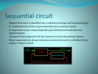
Sequential Models • In digital circuits, storage of data is done either by feedback, or by gate capacitances that are refreshed frequently. Verilog Digital System Design Z. Navabi, 2006
Sequential Models Verilog Digital System Design Z. Navabi, 2006
Feedback Model Verilog Digital System Design Z. Navabi, 2006
Feedback Model A two-state (one-bit) Memory element Feedback Line • Basic Feedback Verilog Digital System Design Z. Navabi, 2006
Capacitive Model Verilog Digital System Design Z. Navabi, 2006
Capacitive Model When c becomes 1 the value of D is saved in the input gate of the inverter and when c becomes 0 this value will be saved until the next time that c becomes 1 again. The complement of the stored data • Capacitive Storage Verilog Digital System Design Z. Navabi, 2006
Implicit Model Verilog Digital System Design Z. Navabi, 2006
Implicit Model Verilog offers language constructs that are technology independent and allow much more efficient simulation of circuits with a large number of storage elements. Feedback and capacitive models are technology dependent and have the problem of being too detailed and too slow to simulate. • An SR-Latch Notation Verilog Digital System Design Z. Navabi, 2006
Basic Memory Components Verilog Digital System Design Z. Navabi, 2006
Gate Level Primitives Gate Level Primitives Verilog Digital System Design Z. Navabi, 2006
Gate Level Primitives 1-bit Storage Element • Cross-Coupled NOR Latch Verilog Digital System Design Z. Navabi, 2006
Gate Level Primitives Base of most static memory components `timescale 1ns/100ps module latch (input s, r, output q, q_b ); nor #(4) g1 ( q_b, s, q ), g2 ( q, r, q_b ); endmodule q and q_b outputs are initially X and remain at this ambiguous state for as long as s and r remain 0. • SR-Latch Verilog Code Simultaneous assertion of both inputs results in loss of memory. Verilog Digital System Design Z. Navabi, 2006
Gate Level Primitives Control Gates Clock Input • All NAND Clocked SR-Latch Verilog Digital System Design Z. Navabi, 2006
Gate Level Primitives Delay values can be controlled when the latch is instantiated. `timescale 1ns/100ps module latch_p #(parameter tplh=3, tphl=5) (input s, r, c, output q, q_b ); wire _s, _r; nand #(tplh,tphl) g1 ( _s, s, c ), g2 ( _r, r, c ), g3 ( q, _s, q_b ), g4 ( q_b, _r, q ); endmodule Set and Reset inputs to the cross_coupled core of this memory element • All NAND Clocked Latch Verilog Digital System Design Z. Navabi, 2006
Gate Level Primitives This delay is due to a fall of 3ns and a rise of 5 ns in the NAND gates of the circuit. • SR Latch Simulation Verilog Digital System Design Z. Navabi, 2006
Gate Level Primitives Master Slave • Master-Slave D Flip-Flop Verilog Digital System Design Z. Navabi, 2006
Gate Level Primitives `timescale 1ns/100ps module master_slave (input d, c, output q, q_b ); wire qm, qm_b; defparam master.tplh=4, master.tphl=4, slave.tplh=4, slave.tphl=4; latch_p master ( d, ~d, c, qm, qm_b ), slave ( qm, qm_b, ~c, q, q_b ); endmodule Hierarchical Naming • Master-Slave D Flip-Flop Verilog Code Verilog Digital System Design Z. Navabi, 2006
User Defined Sequential Primitives Verilog Digital System Design Z. Navabi, 2006
User Defined Sequential Primitives • Verilog provides language constructs for defining sequential UDPs: • Faster Simulation of memory elements • Correspondence to specific component libraries Verilog Digital System Design Z. Navabi, 2006
User Defined Sequential Primitives primitive latch( q, s, r, c ); output q; reg q; input s, r, c; initial q=1'b0; table // s r c q q+ ; // ------:---:----; ? ? 0 : ? : - ; 0 0 1 : ? : - ; 0 1 1 : ? : 0 ; 1 0 1 : ? : 1 ; endtable endprimitive Table defining the latch output • Sequential UDP Defining a Latch Verilog Digital System Design Z. Navabi, 2006
User Defined Sequential Primitives primitive latch( q, s, r, c ); ............. ............. table // s r c q q+ ; // ------:---:----; ? ? 0 : ? : - ; 0 0 1 : ? : - ; 0 1 1 : ? : 0 ; 1 0 1 : ? : 1 ; endtable endprimitive Column for specifying present state Signifies “no change” Signifies “any value” • Sequential UDP Defining a Latch Verilog Digital System Design Z. Navabi, 2006
Memory Elements Using Assignments Memory Elements Using Assignments Verilog Digital System Design Z. Navabi, 2006
Memory Elements Using Assignments When a block’s clock input is 0, it puts its output back to itself (feedback), and when its clock is 1 it puts its data input into its output. • Master-Slave Using Two Feedback Blocks Verilog Digital System Design Z. Navabi, 2006
Memory Elements Using Assignments `timescale 1ns/100ps module master_slave_p #(parameter delay=3) (input d, c, output q); wire qm; assign #(delay) qm = c ? d : qm; assign #(delay) q = ~c ? qm : q; endmodule The feedback of qm output back to its input Each assign statement implements a latch Complementary Clocks: Implements master-slave flip-flop • Assign Statements Implementing Logic Feedback Verilog Digital System Design Z. Navabi, 2006
Behavioral Memory Elements Behavioral Memory Elements Verilog Digital System Design Z. Navabi, 2006
Behavioral Memory Elements • Behavioral Coding: • A more abstract and easier way of writing Verilog code for a latch or flip-flop. • The storage of data and its sensitivity to its clock and other control inputs will be implied in the way model is written. Verilog Digital System Design Z. Navabi, 2006
Behavioral Memory Elements Verilog Digital System Design Z. Navabi, 2006
Latch Modeling Verilog Digital System Design Z. Navabi, 2006
Latch Modeling While c is 1 changes on d directly affect q and q_b outputs. A Storage unit Level Sensitive to c : A Latch `timescale 1ns/100ps module latch (input d, c, outputreg q, q_b ); always @( c or d ) if ( c ) begin #4 q = d; #3 q_b = ~d; end endmodule After 4ns d input is read and assigned to q output. If d changes between the time it is read for q and q_b erroneous results happen. After another wait of 3ns, d is read again and ~d is assigned to q_b output. • A D-Type Latch Verilog Code Verilog Digital System Design Z. Navabi, 2006
Latch Modeling Corrects the timing problem of blocking assignments. `timescale 1ns/100ps module latch (input d, c, output reg q, q_b ); always @( c or d ) if ( c ) begin q <= #4 d; q_b <= #3 ~d; end endmodule Non-blocking assignments With intra-statement delay controls • Latch Model Using Nonblocking Assignments Verilog Digital System Design Z. Navabi, 2006
Latch Modeling • Testing Latch with Nonblocking Assignments Storing a 0 at time 50 Storing a 1 at time 30 Verilog Digital System Design Z. Navabi, 2006
Flip-flop Modeling Verilog Digital System Design Z. Navabi, 2006
Flip-flop Modeling With each clock edge, the entire procedural block is executed once from begin to end. A basic edge trigger flip-flop model at the behavioral level `timescale 1ns/100ps module d_ff (input d, clk, output reg q, q_b ); always @( posedge clk ) begin q <= #4 d; q_b <= #3 ~d; end endmodule Sensitive to the positive edge of the clock Assignments to q and q_b are reached immediately after the flow in always block begins. • Positive Edge Trigger Flip-Flop The actual assignments of values are delayed. Verilog Digital System Design Z. Navabi, 2006
Flip-flop Modeling During the time clk is 1 (from 60ns to 80ns exclusive of 60 and inclusive of 80), changes on d do not affect the state of flip-flop At 60ns, on the positive edge of clock, the value of d is read and scheduled into q and q_b for times 64ns and 63ns respectively. • Simulation of a Positive Edge Flip-Flop Verilog Digital System Design Z. Navabi, 2006
Flip-flop with Set-Reset Control Verilog Digital System Design Z. Navabi, 2006
Flip-flop With Set-Reset Control `timescale 1ns/100ps module d_ff_sr_Synch (input d, s, r, clk, output reg q, q_b ); always @(posedge clk) begin if( s ) begin q <= #4 1'b1; q_b <= #3 1'b0; endelse if( r ) begin q <= #4 1'b0; q_b <= #3 1'b1; end else begin q <= #4 d; q_b <= #3 ~d; end end endmodule • D Type Flip-Flop with Synchronous Control Verilog Digital System Design Z. Navabi, 2006
Flip-flop With Set-Reset Control module d_ff_sr_Synch (input d, s, r, clk, output reg q, q_b ); always @(posedge clk) begin if( s ) begin ................. end else if( r ) begin ................. end else begin ................. end end endmodule The flow into always block is only initiated by the posedge of clk These if-statements with s and r conditions are only examined after the positive edge of the clock Synchronous s and r control inputs • D Type Flip-Flop with Synchronous Control (Continued) Verilog Digital System Design Z. Navabi, 2006
Flip-flop With Set-Reset Control .................. if( s ) begin q <= #4 1'b1; q_b <= #3 1'b0; end else if( r ) begin q <= #4 1'b0; q_b <= #3 1'b1; end else begin q <= #4 d; q_b <= #3 ~d; end .................. These if-statements with s and r conditions are only examined after the positive edge of the clock • D Type Flip-Flop with Synchronous Control (Continued) Verilog Digital System Design Z. Navabi, 2006
Flip-flop With Set-Reset Control `timescale 1ns/100ps module d_ff_sr_Asynch (input d, s, r, clk, outputreg q, q_b ); always @( posedge clk, posedge s, posedge r ) begin if( s ) begin q <= #4 1'b1; q_b <= #3 1'b0; end else if( r ) begin q <= #4 1'b0; q_b <= #3 1'b1; end else begin q <= #4 d; q_b <= #3 ~d; end end endmodule • D-type Flip-Flop with Asynchronous Control Verilog Digital System Design Z. Navabi, 2006
Flip-flop With Set-Reset Control module d_ff_sr_Asynch (input d, s, r, clk, outputreg q, q_b ); always @( posedge clk, posedge s, posedge r ) begin if( s ) begin .................... end else if( r ) begin .................... end else begin .................... end end endmodule The sensitivity list of the always block Asynchronous set and reset inputs • D-type Flip-Flop with Asynchronous Control (Continued) Verilog Digital System Design Z. Navabi, 2006
Flip-flop With Set-Reset Control .................... if( s ) begin q <= #4 1'b1; q_b <= #3 1'b0; end else if( r ) begin q <= #4 1'b0; q_b <= #3 1'b1; end else begin q <= #4 d; q_b <= #3 ~d; end .................... This flip-flop is sensitive to the edge of clock, but to the levels of s and r . • D-type Flip-Flop with Asynchronous Control (Continued) Verilog Digital System Design Z. Navabi, 2006
Flip-flop With Set-Reset Control Before 120 ns, changes to q is triggered by the clock and q_Synch and q_Asynch are the same. s and r become active and cause changes to the flip-flop output. q_Asynch changes occur independent of the clock when s or r becomes active • Comparing Synchronous and Asynchronous Flip-Flop Controls q_Synch will waits for the edge of the clock to set or reset Verilog Digital System Design Z. Navabi, 2006
Other Storage Element Modeling Styles Verilog Digital System Design Z. Navabi, 2006
Other Storage Element Modeling Styles A latch using a wait statement instead of an event control statement `timescale 1ns/100ps module latch (input d, c, outputreg q, q_b ); always begin wait ( c ); #4 q <= d; #3 q_b <= ~d; end endmodule Blocks the flow of procedural block when c is 0. If c becomes 1 and remains at this value, the body of the always statement repeats itself every 7 ns. If the delay control statements are omitted, then the looping of the always block happens in zero time, causing an infinite loop in simulation. • Latch Using wait, a Potentially Dangerous Model Verilog Digital System Design Z. Navabi, 2006
Flip-flop Timing Flip-flop Timing Verilog Digital System Design Z. Navabi, 2006
Flip-flop Timing Verilog Digital System Design Z. Navabi, 2006
Setup Time Verilog Digital System Design Z. Navabi, 2006
Setup Time • Setup Time • The Minimum necessary time that a data input requires to setup before it is clocked into a flip-flop. • Verilog construct for checking the setup time: $setup task • The $setup task: • Takes flip-flop data input, active clock edge and the setup time as its parameters. • Is used within a specify block. Verilog Digital System Design Z. Navabi, 2006
Continuously checks timing distance between changes on d and the positive edge of clk. If this distance is less than 5ns, a violation message will be issued. Setup Time $setup task within a specify block `timescale 1ns/100ps module d_ff ( input d, clk, s, r, output reg q, q_b ); specify $setup ( d, posedge clk, 5 ); endspecify always @( posedge clk orposedge s or posedge r ) begin .............. end endmodule Positive edge trigger flip-flop and Asynchronous set and reset controls • Flip-Flop with Setup Time Verilog Digital System Design Z. Navabi, 2006