Sequential Circuit Design
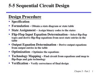
Sequential Circuit Design. Sequential Circuit Design . Start : With a list of specifications End : With a logic diagram OR list of boolean functions # FFs to be used depends on the # of states. At most 2 n states can be represented with n FFs. Sequential circuit design Procedure.


Sequential Circuit Design
E N D
Presentation Transcript
Sequential Circuit Design • Start: With a list of specifications • End: With a logic diagram OR list of boolean functions • # FFs to be used depends on the # of states. At most 2n states can be represented with n FFs. asep@stmik-raharja.com
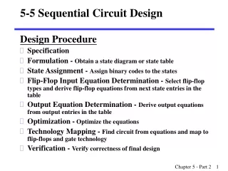
Sequential circuit design Procedure • The design procedure consists of the following steps: • Given the problem statement, derive either the state table or state diagram. • Derive the state table (if not derived in 1). • (optional) Apply state-reduction methods to reduce (if possible) the number of states. • Assign binary values to each state if the state table obtained in Step 2 or 3 contains letter symbols (state assignment) to derive the encoded state table. asep@stmik-raharja.com
Sequential circuit design Procedure (cont.) • Determine the number of flip flops needed and the type of flip-flop to be used. • Derive the flip-flop input equations from next state entries in the encoded state table. • Derive the circuit output functions from the output entries in the encoded state table. • Simplify the flip-flop input equations and output equations using K-map or other simplification methods. • Draw the logic diagram. asep@stmik-raharja.com
Example 1: Find the state diagram and table of a Sequence Recognizer • Design a single-input (X), single-output (Y) synchronous sequence detector. • Every time a pattern of sequence 0101 is detected, this sequence detector produces an output Y = 1; otherwise, Y = 0. • For example, when the input sequence is 01010100, the corresponding output sequence is 00010100. asep@stmik-raharja.com
Example 1 (cont.) • We can construct the state diagram of the detector with four states: A, B, C, and D. • Why four? What do they mean? • A: ground zero; we don’t have any of the desired sequence. • B: just got the leading 0 • C: just got 01 • D: just got 010 • If we’re in state D and we see ‘1’ on X, we set the output Y=1. asep@stmik-raharja.com
Example 1: State Diagram 0/0 asep@stmik-raharja.com
Example 1: State table asep@stmik-raharja.com
Example 1: State table (cont.) • Alternatively: asep@stmik-raharja.com
Example 1 (cont.) • Step 3: (state minimization; strictly optional). It is impossible to reduce the number of states in this example. • If A and B are equivalent, A and C must be equivalent, which implies B and D are equivalent. The latter (B and D are equivalent) is not true, and hence A and B are NOT equivalent. We may apply the argument above to all pairs of states to find out that no two states are equivalent. asep@stmik-raharja.com
Example 1 (cont.) • Step 4 (state assignment): Assign binary codes to each state. • Since we have four states, we need two state variables, S1 and S0, and the values assigned to the four states are 00 A, 01 B,10 C, 11 D. asep@stmik-raharja.com
Example 1: Encoded State table asep@stmik-raharja.com
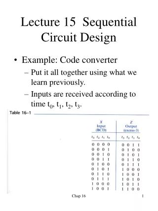
Example 2: BCD-to-Excess 3 Decoder • Find the state diagram and state table of a Binary-Coded-Decimal to Excess-3 decoder. • Recall the truth table for the corresponding combinational circuit shown on the right. BCD code is loaded in parallel Excess-3 code is produced in parallel Comb. Circuit A W B X C Y D Z asep@stmik-raharja.com
Example 2: BCD-to-Excess 3 Decoder (cont.) • An alternative design is a synchronous sequential circuit with 1 input and 1 output. The BCD code is loaded serially, LSB first, and the Excess-3 code is also produced serially, again with LSB first. • To derive such a circuit, we rearrange the truth table of the combinational circuit to help us derive the state diagram. asep@stmik-raharja.com
Sequence of values for single input I Sequence of values for single output O Primary Inputs Primary Outputs Example 2: Rearrange Table Table Transformation: Start with LSB first asep@stmik-raharja.com
Example 2: Rearrange Table Table Transformation Again: Sort the last table in order of common prefixes asep@stmik-raharja.com
Example 2: BCD-to-Excess 3 Decoder (cont.) • Now we are ready to use the last derived table to find the corresponding state diagram. • Remember, output O depends on input I and present state. • Also, the circuit MUST be ready to receive a new 4-bit input sequence as soon as the prior sequence is complete. asep@stmik-raharja.com
ID=1 0/0, 1/1 IC=X Example 2: State Diagram (cont.) Why does this occur? ID=1 ID=1 0/0 1/1 0/0, 1/1 IC=0 IC=1 IC=X 0/1 1/0 0/1 1/0 0/1 1/0 IB=0 IB=1 IB=0 IB=1 IB=0 IB=1 Subgraphs are isomorphic, i.e., same transitions lead to same next states. This is redundant and can be eliminated by collapsing the two current states into one asep@stmik-raharja.com