Download
1 / 26
270 likes | 305 Vues
Learn how to design sequential circuits and code converters with practical examples. Understand state tables, graph construction, state reduction, and state assignment. Explore the implementation of sequential circuits using ROMs, PLAs, CPLDs, and FPGAs. Delve into simulations, delays, synchronizer circuits, and more.

E N D
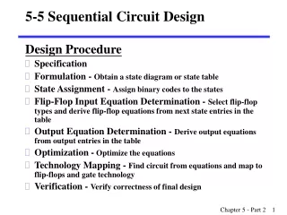
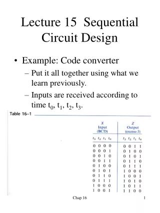
Lecture 15 Sequential Circuit Design • Example: Code converter • Put it all together using what we learn previously. • Inputs are received according to time t0, t1, t2, t3. Chap 16
Code Converter • State table construction: least significant bit is received first. • At t1, starting with B = 0, if the network receives X = 0, we call state D. This means 00 is received. We should give Z = 1 for input X = 0. (Check Table 16-1 for all 00s, we have Z=1 at t1). For input = 0, output = 1 (Check T 16-1 at t0) Chap 16
Code Converter (cont.) • Or construct the state graph first. • Starting at t3, path 0000 has outputs 0011 as given in Table 16-1. Chap 16
Code Converter (cont.) • State reduction: find the equivalent states. Chap 16
Code Converter (cont.) • State assignment • State B and C, D and E, H and M should be given adjacent assignments. • State A,B,E,M, state C, D, and H should be given adjacent assignments. G3. (Output) Chap 16
Code Converter (cont.) • Find the Q+ map, and then the FF input equations. Chap 16
Iterative Circuits • Same operation in each cell. • Parallel inputs/parallel outputs • Combinational cells • Primary inputs Xi • Primary output Zi • Secondary input ai • Secondary output a i+1 Chap 16
A Comparator • Compare two binary numbers • X = x1x2….xn and Y = y1y2y3.. yn • The left bit is the most significant bit. • Comparison proceeds from left to right. • To the left of cell i, either X=Y, X>Y, or X<Y These input conditions called S0, S1, S2 S i+1 is output state at the right of cell i with the input xi yi and the input state at the left of the cell (Si) Si Si+1 Chap 16
A Cell in the Comparator • State assignment Chap 16
End Cells in the Comparator • For the left end cell, a1= b1 = 0. Can be used to simplify the equation for this cell. • Output Z1 (X < Y) = 1 (S2 = 10 = a n+1 b n+1), 11 is not used. Chap 16
Sequential Circuit Version • Inputs are received serially. • Use the same table (state table) • The same next state equations. Chap 16
Sequential Circuits Using ROMs • ROM for combinational parts • 7 states: 3 D FFs => 4 outputs/4 inputs Chap 16
Sequential Circuits Using ROMs • ROM for combinational parts • 7 states: 3 D FFs => 4 outputs/4 inputs Q+ Address bus Data bus Chap 16
Sequential Circuits Using PLAs • For PLA, this table uses 4 inputs/4 outputs, 13 products terms (excluding xxxx) PLA Chap 16
Sequential Circuits Using PLAs • For PLA, this table uses 4 inputs/4 outputs and 7 product terms. (Fig 16-2 assignment) Chap 16
PALs for Sequential Circuit • Programmable AND array. • Q+ = D = A’BQ’ + AB’Q Chap 16
CPLDs for Sequential Circuit • CPLD = function blocks + MCs + AIM + I/Os + etc • PLA in each function block • AIM: advanced interconnection matrix • Macocell = MUXs + FFs (or latches) • Dual-edge triggered FF Chap 16
A Macrocell Product terms • CPLD Logic 1 (get OR’) Logic 0 (pass OR) OR array AND array Invert clock D or T or S-R Chap 16
CPLDs for Sequential Circuit • CPLD for a Mealy machine • 4 macrocells • Two for D FF inputs • Two for output Z AIM Chap 16
FPGAs for Sequential Circuit • FPGA = configurable logic blocks (CLB) + I/O blocks + (memory blocks + CLK generators + tri-state buffers) • CLB = LUTs + MUXes + D-CE FFs • I/O block = FFs (for I/O) + tri-state buffers Chap 16
FPGAs for Sequential Circuit • FPGA for a Mealy machine • FG: functional generator Chap 16
Simulations • Functional level • Sequence of transfers btw registers, ALU, memories. • Verify high level system design • Logic level • Logic gates, FF, and interconnection • Verify logic design and analyze timing • Circuit level • Each gate is represented in transistors, R, C. • Information about voltage level and switching speed. Chap 16
Delays • Unit delay model for simulation at first. • Minimum – Nominal- Maximum delay • Shaded area indicates that B may change at any time during this interval. Chap 16
Synchronizer Circuits • Purpose: Synchronize the inputs w.r.t. clock. • X1s and X2s always change immediately following the clock pulse. Inputs are loaded into the shift register and use the same clock to shift one at a time Chap 16
Synchronizer Circuits • This synchronizer may fail if the FF enters the metastable state. • When the signal that is sampled is not stable for the required set-up time and hold time. The FF may go into a metastable state where the output will not have a legitimate high or low value, but in an indeterminate region between them. • The FF can not be guaranteed to exit the metastable in any bounded time. But the probability of the FF in the metastable state decreases exponentially with time. • So, the solution is to wait more time until the output is stable. Chap 16
Synchronizer Circuits • This synchronizer will work properly if the period of metastability is less than the clock period. • The first output of the D FF may be metastable, it will not be seen by other logic element until the second clock, when the second D FF samples the signal, which by that time should no longer be in a metastable state. It does not matter whether X1s is delayed for one or two clocks. Chap 16