Download

1 / 53
550 likes | 631 Vues
Learn about sequential circuits, latches, flip-flops, state minimization, timing, and design examples from Dr. Aiman H. El-Maleh at King Fahd University. Understand circuit models, behaviors, and design procedures in this comprehensive course outline.

E N D
COE 405Sequential Circuit Design Dr. Aiman H. El-Maleh Computer Engineering Department King Fahd University of Petroleum & Minerals
Outline • Sequential Circuit Model • Timing of Sequential Circuits • Latches and Flip flops • Sequential Circuit Design Procedure • Sequential Circuit Design Examples • State Minimization • State Encoding • Sequential Circuit Timing
Sequential Circuit Model • A Sequential circuit consists of: • Data Storage elements: (Latches / Flip-Flops) • Combinatorial Logic: • Implements a multiple-output function • Inputs are signals from the outside • Outputs are signals to the outside • State inputs (Internal): Present State from storage elements • State outputs, Next State are inputs to storage elements
Sequential Circuit Model • Combinatorial Logic • Next state function: Next State = f(Inputs, State) • 2 output function types : Mealy & Moore • Output function: Mealy Circuits Outputs = g(Inputs, State) • Output function: Moore Circuits Outputs = h(State) • Output function type depends on specification and affects the design significantly
Sequential Circuit Model Mealy Circuit Moore Circuit
Timing of Sequential CircuitsTwo Approaches • Behavior depends on the times at which storage elements ‘see’ their inputs and change their outputs (next state present state) • Asynchronous • Behavior defined from knowledge of inputs at any instant of time and the order in continuous time in which inputs change • Synchronous • Behavior defined from knowledge of signals at discrete instances of time • Storage elements see their inputs and change state only in relation to a timing signal (clock pulses from a clock) • The synchronous abstraction allows handling complex designs!
Set-Reset Latch & Flip Flop Nor-Nor SR Latch Nand-Nand SR Latch Master-Slave SR Flip-Flop Clocked SR Latch
D Latch & D Flip Flop D Latch Rising-Edge Triggered D Flip Flop
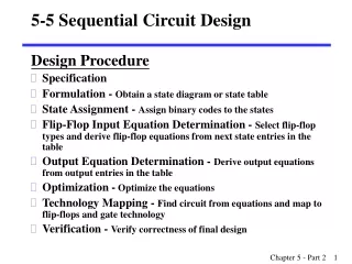
Sequential Circuit Design Procedure • 1. Specification – e.g. Verbal description • 2. Formulation – Interpret the specification to obtain a state diagram and a state table • 3. State Assignment - Assign binary codes to symbolic states • 4. Flip-Flop Input Equation Determination - Select flip-flop types and derive flip-flop input equations from next state entries in the state table • 5. Output Equation Determination - Derive output equations from output entries in the state table • 6. Verification - Verify correctness of final design
State Initialization • When a sequential circuit is turned on, the state of the flip flops is unknown (Q could be 1 or 0) • Before meaningful operation, we usually bring the circuit to an initial known state, e.g. by resetting all flip flops to 0’s • This is often done asynchronously through dedicated direct S/R inputs to the FFs • It can also be done synchronously by going through the clocked FF inputs
Example: Bit Sequence Recognizer 1101 • 1. Specifications: Detect the occurrence of bit sequence 1101 whenever it occurs on input X and indicate this detection by raising an output Z high • 2. Formulation: State Diagram
Example: Bit Sequence Recognizer 1101 • From the State Diagram, we can fill in the 2-D State Table • There are 4 states, one input, and one output. • Two dimensional table with four rows, one for each current state. State Table State Diagram
Example: Bit Sequence Recognizer 1101 • 3. State Assignment: From abstract symbols to binary bit representation of states • Each of the m symbolic states must be assigned a unique binary code • Minimum number of state bits (state variables) (FFs) required is nb, such that 2nb ≥ ns • If 2nb > ns, this leaves (2nb – ns) unused states • Utilize them as don’t care conditions to simplify CL design • But may need caution: e.g. what if the circuit enters an unused state by mistake nb= log2 ns.
Example: Bit Sequence Recognizer 1101 • Also which code is given to which state? different CL implementations may influence optimization, e.g. (with 2 FFs) State A is assigned 00 or 01 or 10 or 11? • There are possible encodings = 16 • Let A = 00 (to suit being a Reset state), B = 01, C = 11, D = 10
Example: Bit Sequence Recognizer 1101 • For optimization of FF input equations we express A(t+1), B(t+1), Z(t) in terms of A(t), B(t) and X(t) (using one dimensional state table)
BCD to Excess-3 Serial Code Converter • Assume that once the machine is reset, a continues stream of BCD digits will be transmitted serially and converted to Excess-3 digits.
BCD to Excess-3 Serial Code Converter State Diagram State Table
BCD to Excess-3 Serial Code Converter Karnaugh maps for the encoded state bits and output bit (Bout)
Serial-Line Code Converter for Data Transmission • Line codes are used in data transmission or storage systems to reduce effects of noise in serial communication channels. • Receiver of data must be able to operate synchronosly with sending unit. • Code converters transform data stream into a format encoded to enable receiver to recover data. • A phase lock loop (PLL) can recover clock from line data • If no long series of 1’s or 0’s in data encoded in non-return-to-zero (NRZ) format • If no long series of 0’s in data encoded in non-return-to-zero invert-on-ones (NRZI) format or return-to-zero (RZ) format • Always for Manchester format.
Serial-Line Code Converter for Data Transmission • NRZ Code: duplicates the bit pattern of the input signal • NRZI Code: the output remains constant as long as the input is 0 and toggles if the input is 1. • RZ Code: a 0 is transmitted as a 0, while a 1 is transmitted as a 1 for the first half of the bit time and a 0 for the remaining bit time. • Manchester Code: a 0 is transmitted as a 0 for the first half of the bit time and a 1 for the remaining bit time, while a 1 is transmitted as a 1 for the first half of the bit time and a 0 for the remaining bit time.
NRZ to Manchester Code Converter Note that clock_2 has twice the clock frequency of clock_1
State Minimization • Aims at reducing the number of machine states • reduces the size of transition table. • State reduction may reduce • the number of storage elements. • the combinational logic due to reduction in transitions. • Completely specified finite-state machines • No don't care conditions. • Easy to solve. • Incompletely specified finite-state machines • Unspecified transitions and/or outputs. • Intractable problem.
State Minimization for Completely-Specified FSMs • Equivalent states • Given any input sequence the corresponding output sequences match. • Theorem: Two states are equivalent iff • they lead to identical outputs and • their next-states are equivalent. • Equivalence is transitive • Partition states into equivalence classes. • Minimum finite-state machine is unique.
State Minimization Algorithm • Stepwise partition refinement. • Initially • 1 = States belong to the same block when outputs are the same for any input. • Refine partition blocks: While further splitting is possible • k+1 = States belong to the same block if they were previously in the same block and their next-states are in the same block of k for any input. • At convergence • Blocks identify equivalent states.
State Minimization Example • 1 = {(s1, s2), (s3, s4), (s5)}. • 2 = {(s1, s2), (s3), (s4), (s5)}. • 2 = is a partition into equivalence classes • States (s1, s2) are equivalent.
State Minimization Example Original FSM Minimal FSM
State Minimization Example Original FSM {OUT_0} = IN_0 LatchOut_v1' + IN_0 LatchOut_v3' + IN_0' LatchOut_v2' v4.0 = IN_0 LatchOut_v1' + LatchOut_v1' LatchOut_v2' v4.1 = IN_0' LatchOut_v2 LatchOut_v3 + IN_0' LatchOut_v2' v4.2 = IN_0 LatchOut_v1' + IN_0' LatchOut_v1 + IN_0' LatchOut_v2 LatchOut_v3 sis> print_stats pi= 1 po= 1 nodes= 4 latches= 3 lits(sop)= 22 #states(STG)= 5 Minimal FSM {OUT_0} = IN_0 LatchOut_v1' + IN_0 LatchOut_v2 + IN_0' LatchOut_v2' v3.0 = IN_0 LatchOut_v1' + LatchOut_v1' LatchOut_v2‘ v3.1 = IN_0' LatchOut_v1' + IN_0' LatchOut_v2' sis> print_stats pi= 1 po= 1 nodes= 3 latches= 2 lits(sop)= 14 #states(STG)= 4
Input Next State Output Sequence Present State X=0 X=1 X=0 X=1 Reset S0 S1 S2 0 0 0 S1 S3 S4 0 0 1 S2 S5 S6 0 0 00 S3 S0 S0 0 0 01 S4 S0 S0 1 0 10 S5 S0 S0 0 0 11 S6 S0 S0 1 0 S0 0/0 1/0 S1 S2 0/0 1/0 0/0 1/0 S3 S4 S5 S6 1/0 1/0 1/0 1/0 0/0 0/1 0/0 0/1 Another State Minimization Example • Sequence Detector for codes of symbols 010 or 110 assuming that each symbol code is 3 bits in length
Input Next State Output Sequence Present State X=0 X=1 X=0 X=1 Reset S0 S1 S2 0 0 0 S1 S3 S4 0 0 1 S2 S5 S6 0 0 00 S3 S0 S0 0 0 01 S4 S0 S0 1 0 10 S5 S0 S0 0 0 11 S6 S0 S0 1 0 Another State Minimization Example ( S0 S1 S2 S3 S4 S5 S6 ) ( S0 S1 S2 S3 S5 ) ( S4 S6 ) ( S0 S3 S5 ) ( S1 S2 ) ( S4 S6 ) ( S0 ) ( S3 S5 ) ( S1 S2 ) ( S4 S6 ) S1 is equivalent to S2 S3 is equivalent to S5 S4 is equivalent to S6
Input Next State Output Sequence Present State X=0 X=1 X=0 X=1 Reset S0 S1' S1' 0 0 0 + 1 S1' S3' S4' 0 0 X0 S3' S0 S0 0 0 X1 S4' S0 S0 1 0 S0 X/0 S1’ 0/0 1/0 S4’ S3’ X/0 0/1 1/0 Another State Minimization Example • State minimized sequence detector for 010 or 110
00 10 S0[1] S1 [0] 00 01 10 11 11 01 00 01 00 S2[1] S3 [0] 01 10 10 11 11 01 10 10 S4[1] S5 [0] 11 00 00 01 11 Multiple Input Example present next state output state 00 01 10 11 S0 S0 S1 S2 S3 1 S1 S0 S3 S1 S4 0 S2 S1 S3 S2 S4 1 S3 S1 S0 S4 S5 0 S4 S0 S1 S2 S5 1 S5 S1 S4 S0 S5 0
present next state output state 00 01 10 11 S0' S0' S1 S2 S3' 1 S1 S0' S3' S1 S0’ 0 S2 S1 S3' S2 S0' 1 S3' S1 S0' S0' S3' 0 S1 S0-S1 S1-S3 S2 S3-S4 S0-S1 S3-S0 S3 S1-S4 minimized state table (S0==S4) (S3==S5) S4-S5 S1-S0 S3-S1 S4 S4-S5 S0-S1 S3-S4 S5 S4-S5 S0 S1 S2 S3 S4 Implication Chart Method • Cross out incompatible states based on outputs • Then cross out more cells if indexed chart entries are already crossed out present next state output state 00 01 10 11 S0 S0 S1 S2 S3 1 S1 S0 S3 S1 S4 0 S2 S1 S3 S2 S4 1 S3 S1 S0 S4 S5 0 S4 S0 S1 S2 S5 1 S5 S1 S4 S0 S5 0 S3-S5 S0-S4
State Minimization Computational Complexity • Polynomially-bound algorithm. • There can be at most |S| partition refinements. • Each refinement requires considering each state • Complexity O(|S|2). • Actual time may depend upon • Data-structures. • Implementation details.
State Encoding • Determine a binary encoding of the states (|S|=ns) that optimize machine implementation • Area • Cycle-time • Power dissipation • Testability • Assume D-type registers. • Circuit complexity is related to • Number of storage bits nb used for state representation • Size of combinational component • There are possible encodings • Implementation Modeling • Two-level circuits. • Multiple-level circuits.
Timing Constraints • TD= worst case delay through combinational logic • TSU = FF set up time – Minimum time before the clock edge where the input data must be ready and stable • TclkQ = Clock to Q delay – Time between clock edge and data appearing at the output of the FF • THold= FF hold time – Minimum time after the clock edge where data has to remain stable (held stable) • Based on the FF & combinational logic timing parameters, the following timing constraints are obtained for correct operation of the circuit: Tclk ≥ Tclkq1 + TD + Tsu
Timing Constraints • The previous equation assumes that the clock arrives at all FFs, at exactly the same time! • Clock Skew (Tskew) is the delay between clocks at different chip locations. • To take Clock Skew into account: Tclk≥ Tclkq1+ TD+ Tsu+ Tskew • Clock Signals will have random variations in their Periods and Frequencies, called Jitter. • The latest arrival time minus the earliest arrival time during an observed period of time is called the "peak to peak jitter amplitude". • We have to take the Peak to Peak Jitter (TP-P Jitter) into account Tclk≥ T clkq1+ TD+ Tsu+ Tskew+ TP-P Jitter