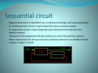
Sequential Circuit Timing
Sequential Circuit Timing. Objectives This section covers several timing considerations encountered in the design of synchronous sequential circuits. It has the following objectives:

Sequential Circuit Timing
E N D
Presentation Transcript
Sequential Circuit Timing • Objectives This section covers several timing considerations encountered in the design of synchronous sequential circuits. It has the following objectives: • Define the following global timing parameters and show how they can be derived from the basic timing parameters of flip-flops and gates. • Maximum Clock Frequency • Maximum allowable clock skew • Global Setup and Hold Times • Discuss ways to control the loading of data into registers and show why gating the clock signal to do this is a poor design practice.
Reading Assignment • Much of the information in this section is not in the Brown & Vranesic text. There is material on clock skew in section 10.3. That section also discusses the effects of gating the clock.
13.1. Maximum Clock Frequency • The clock frequency for a synchronous sequential circuit is limited by the timing parameters of its flip-flops and gates. This limit is called the maximum clock frequency for the circuit. The minimum clock period is the reciprocal of this frequency. • Relevant timing parameters • Gates: • Propagation delays: min tPLH, min tPHL, max tPLH, max tPHL • Flip-Flops: • Propagation delays: min tPLH, min tPHL, max tPLH, max tPHL • Setup time: tsu • Hold time: th
Example TW ≥ max tPFF + tsu • For the 7474, max tPLH = 25ns, max tPHL = 40ns, tsu = 20ns • TW ≥ max (max tPLH + tsu, max tPHL + tsu) • TW ≥ max (25+20, 40+20) = 60
Example TW ≥ max tPFF + max tPINV + tsu
Example TW ≥ max tPFF + max tPMUX + tsu
Example Paths from Q1 to Q1: None Paths from Q1 to Q2: TW ≥ max tPDFF +tJKsu = 20 +10 = 30 ns TW ≥ max tPDFF + max tAND + tJKsu = 20 + 12 + 10 = 42 ns Paths from Q2 to Q1: TW ≥ max tPJKFF + tOR + TDsu = 25 + 10 + 5 = 40 ns TW ≥ max tPJKFF + max tAND + tJKsu = 25 + 12 + 10 = 47 ns Paths from Q2 to Q2: TW ≥ 47 ns
Clock Skew • If a clock edge does not arrive at different flip-flops at exactly the same time, then the clock is said to be skewed between these flip-flops. The difference between the times of arrival at the flip-flops is said to be the amount of clock skew. • Clock skew is due to different delays on different paths from the clock generator to the various flip-flops. • Different length wires (wires have delay) • Gates (buffers) on the paths • Flip-Flops that clock on different edges (need to invert clock for some flip-flops) • Gating the clock to control loading of registers (a very bad idea)
Example (Effect of clock skew on clock rate) • Clock C2 skewed after C1 TW ≥ max TPFF + max tOR + tsu (if clock not skewed, i.e., tINV = 0) TW ≥ max TPFF + max tOR + tsu - min tINV (if clock skewed, i.e., tINV > 0)
Clock C1 skewed after C2 TW ≥ max TPFF + max tOR + tsu (if clock not skewed, i.e., tINV = 0) TW ≥ max TPFF + max tOR + tsu + max tINV (if clock skewed, i.e., tINV > 0)
Summary of maximum clock frequency calculations C2 skewed after C1: TW ≥ max TPFF + max tNET + tsu - min tINV C2 skewed before C1: TW ≥ max TPFF + max tNET + tsu + max tINV
Example • For each of the following two connections find • The minimum clock period • The maximum and minimum delay from CLK to YOUT
Circuit 1: n ≥ 2 Minimum Clock Period: Tw ≥ max tPFF + max tQY + (n-2) max tXY +max tXD + tsu ≥ TW Tw ≥ max tPFF + max tQD + tsu Maximum Delay: TCY ≤ max tPFF + max tQY + (n-1) max tXY Minimum Delay: TCY ≥ min tPFF + min tQY
Circuit 2: n ≥ 2 Minimum Clock Period: Tw ≥ max tPFF + max tXD + tsu Tw ≥ max tPFF + max tQD + tsu Maximum Delay: TCY ≤ max tPFF + max (max tXY,max tQY) Minimum Delay: TCY ≥ min tPFF + min (min tXY, min tQY)
2. Maximum Allowable Clock Skew • How much skew between C1 and C2 can be tolerated in the following circuit? • Case 1: C2 delayed after C1 tPFF > th + tSK tSK < min tPFF - th
How does additional delay between the flip-flops affect the skew calculations? tSK ≤ min tPFF - th tsk ≤ min tPFF + min tMUX - th
Summary of allowable clock skew calculations tSK + th ≤ tPFF + tNET tSK ≤ min tPFF + min tNET - th
Example: What is the minimum clock period for the following circuit under the assumption that the clock C2 is skewed after C1 (i.e., C2 is delayed from C1)?
First calculate the maximum allowable clock skew. • Next calculate the minimum clock period due to the path from Q1 to D2. • Finally calculate the minimum clock period due to the path from Q2 to D1 tSK < min tPFF + min tN1 - th TW > max tPFF + max tN1 + tsu - min tSK TW > max tPFF + max tN2 + tsu + max tSK TW > max tPFF + max tN2 + tsu + (min tPFF + min tN1 - th) TW > max tPFF + min tPFF + max tN2 + min tN1 + tsu - th
3. Global Setup Time, Hold Time and Propagation Delay • Global setup and hold times (data delayed) TH = th - min tNET TSU = tsu + max tNET
Global setup & hold time (clock delayed) TSU = tsu - min tC TH = th + max tC
Global setup & hold time (data & clock delayed) TSU = tsu + max tNET - min tC TH = th - min tNET + max tC
Global propagation delay TP = tC + tFF + tNET
Summary of global timing parameters TSU = tsu + max tPN - min tPC ≤ tsu + max tPN TH = th + max tPC - min tPN ≤ th + max tPC TP = tPFF + tPN + tPC
Example • Find TSU and TH for input signal LD relative to CLK. TSU = tsu +max tNET - min tC = tsu + max tINV + max tNAND + max tNAND - min tINV TH = th - min tNET + max tC = th - min tNAND - min tNAND + max TINV
4. Register load control (gating the clock) • A very bad way to add a load control signal LD to a register that does not have one is shown below • The reason this is such a bad idea is illustrated by the following timing diagram. • The flip-flop sees two rising edges and will trigger twice. The only one we want is the second one.
If LD was constrained to only change when the clock was low, then the only problem would be the clock skew.
If gating the clock is the only way to control the loading of registers, then use the following approach: • There is still clock skew, but at least we only have one triggering edge.
6. Review • How the flip-flop and gate timing parameters affect the maximum possible clock frequency. • How clock skew affect maximum possible clock frequency. • How the delay of logic between flip-flops affects the maximum allowable clock skew. • How flip-flop setup and hold times are translated by the combinational logic delays to get global setup and hold times. • The detrimental effect of gating the clock signal.
Extra Timing Problems • The following logic diagram shows the implementation of the ith bit slice of a register. Derive the global setup and hold times TSU and TH for CLR and the maximum and minimum propagation delays max TP and min TP from CLK to the flip-flop outputs. Use the following timing parameters. JK Flip-Flop: 5ns ≤ tPFF ≤ 15ns tsu = 12ns th = 6ns NAND Gate: 3ns ≤ tPNAND ≤ 10ns Inverter: 2ns ≤ tPINV ≤ 8ns
Determine the minimal clock period TW for the following circuit. Use the following delay values for the flip-flops and gates. • Flip-Flop: 5 ≤ tPFF ≤ 14ns; tsu = 6ns; th = 10ns • Inverter: 2 ≤ tPINV ≤ 12 • XOR Gate: 7 ≤ tXOR ≤ 22 Part a) Work the problem under the assumption that the clock is symmetrical. That is, it is high for 50% of the clock period and low for 50% of the clock period. Part b) Work the problem under the assumption that the clock is high for 20% of the clock period and low for 80% of the clock period.