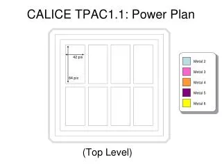
CALICE TPAC1.1: Power Plan
120 likes | 229 Vues
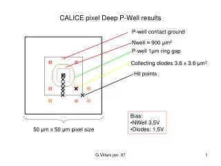
This document provides a detailed overview of the metal layers and power planning strategies used in advanced circuit design. It highlights key aspects such as missing horizontal links between sub-arrays, various voltage supply points (VDD/VSS), and various signal biases. The focus is on the identification of specific pixel rows and columns within the layout, as well as issues related to SRAM and guard voltages. Attention is drawn to necessary revisions and checks required in the design to ensure optimal performance.

CALICE TPAC1.1: Power Plan
E N D
Presentation Transcript
Metal 2 Metal 3 Metal 4 Metal 5 Metal 6 CALICE TPAC1.1: Power Plan 42 pix 84 pix (Top Level)
1.1 VDD1V8pix & VSS:Gpix
1.1 (new mesh) VDD1V8aco & VSS:Gaco
1.1 VDD1V8dco & VSS:Gdco
1.1 (attn!) VDD1V8mso & VSS:Gmso Horizontal links between sub-arrays missing! TO DO
1.1 VDD1V8sram & VSS:Gsram
1.1 VGUARD (not yet used)
1.1 Vth(+/-) & Vcasc(s) Vth12 Vth34 Vcascs, Vbiases
1.1 VDD1V8dig & VSS:Gdig
VDD2V5dig (=3.3v for SRAM WrEn) 1.1 (review)
1 1 2 2 preShape BTBTTB preShape BTBTTB preShape BTBTTB preShape BTBTTB Col 01 Col 00 Col 11 Col 10 Pixel Identification Row 0 Row 1 Row 2 etc [GRAY] Row 83 0,1,2,3 … 42 0,1,2,3 … 42 0,1,2,3 … 42 0,1,2,3 … 42 Row 84 Row 85 Row 86 etc [GRAY] Row 167 0,1,2,3 … 42 0,1,2,3 … 42 0,1,2,3 … 42 0,1,2,3 … 42