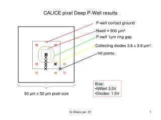
CALICE Pixel Deep P-Well Results: Charge Collection and Layout Comparisons
60 likes | 182 Vues
This document presents the results of the CALICE pixel deep P-well simulations, focusing on charge collection performance and layout effects in pixel designs. The study compares the central N-well (900 μm²) and guard ring configurations under various bias settings, with an emphasis on the impact on collection times and signal-to-noise ratios. It highlights the advantages and limitations of different pixel structures, the influence of ring gaps, and future simulation plans for optimizing diode sizes. Key findings reveal that central N-well layouts perform comparably despite worse charge collection metrics.

CALICE Pixel Deep P-Well Results: Charge Collection and Layout Comparisons
E N D
Presentation Transcript
CALICE pixel Deep P-Well results P-well contact ground Nwell ≈ 900μm2 P-well 1μm ring gap Collecting diodes 3.6 x 3.6 μm2 Hit points • Bias: • NWell 3.5V • Diodes: 1.5V 50 μm x 50 μm pixel size G.Villani jan. 07
CALICE pixel Deep P-Well results P-well contact ground Nwell 3.6 x 3.6 μm2 P-well 1μm ring gap P-well 5μm guard ring Collecting diodes 3.6 x 3.6 μm2 1 μm clearance from the guard ring Hit point • Bias: • NWell 3.5V • Diodes: 1.5V 50 μm x 50 μm pixel size G.Villani jan. 07
≈ 9.5 μm ≈ 202 mV ≈ 144 mV CALICE pixel Deep P-Well results Deep P Well Ring ( @ z= 31 μm) Epitaxial layer potential well μm V top μm G.Villani jan. 07
e- 1 6 CALICE pixel Deep P-Well simulation results Single pixel results Pwell Guard ring and CNW comparison CNW: 257 (e- ) GR: 268 (e- ) Guard Ring DPW Central NW 900 um2 Diodes Charge collected (e- ) G.Villani jan. 07 CNW Charge collected (e- ) Collection time (ns)
CALICE pixel Deep P-Well results • Conclusions • The layout with central well size 900 μm2 clearly shows worse performances in terms of charge collection compared to the guard ring PW: however the worst cases seem comparable, suggesting a S/Nmin exceeding 10 in both cases • Collection time still well below 200 ns in both cases, with central NW 900 μm2 faster than the guard ring PW. • Shielding effect P Well Guard ring has to be assessed with reference to similar layouts: no NW strips WERE present in the 5 μm guard ring layout, that might affect charge collection by the diodes. • Next step: • Final layout simulation with and without 3 μm PW guard ring and proper biasing • Different size diodes simulations (7.6 / 1.8 μm) G.Villani jan. 07
CALICE pixel Deep P-Well results Narrow ( 3 μm ?) P-Well guard ring around each pixel G.Villani jan. 07