Progress Meeting Highlights: Tera-Pixel APS for CALICE Project
Discussion on Foundry and Rutherford actions, including process splits, IO pad libraries, and charge amplifier design, for the Tera-Pixel APS project. Detailed insights and future plans shared.

Progress Meeting Highlights: Tera-Pixel APS for CALICE Project
E N D
Presentation Transcript
Tera-Pixel APS for CALICE Progress meeting, 12th July 2006 Jamie Crooks, Microelectronics/RAL
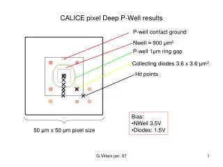
Phone meeting with Foundry (June 19th) • Foundry Actions: • Check the possibility of performing process splits in Shuttle run • Check the availability of the corner model for Deep N-well Diode - dnwell33 • Check the availability of the GDS files of the following IO pad libraries: • staggered analog pads • PCI inline pads • Check if Foundry offers large IO pads (100um x 100um) both for Analog and Digital • Send Rutherford the shuttle schedule for the beginning of 2007 • Rutherford Actions: • Send Foundry a draft of Calice project • Send Foundry Rutherford’s requirements for TCAD tool both for MI3 and Calice projects. • Fill out and send Foundry the CIS Application General Questionnaire for Calice project (see attached) Yes this is possible • No model avail. pending Sent example pixel GDS Sent summary document (details from Guilio)
Analog Pixel • Voltage amplifiers disappointing • Charge amplifiers may be more appropriate • Autozero comparator may be too complex • Clock line switching in every pixel • Simpler comparator design possible if we can reset the pixel after a hit?
Charge Amplifier • Smaller Cfb Larger output step • Charge-to-voltage gain is independent of Cd (hence can have 4 diodes in parallel) Larger voltage step at output than seen before • Purely capacitive feedback requires a reset phase • Diode feedback provides resistive ‘biasing’ feedback • No corner of MonteCarlo models for diode • Parasitic feedback subject to layout and accuracy of 3D parasitic extraction tools! Vout Cfb Cd
Charge Amplifiers Vout Vout Vout Diode feedback Capacitor feedback Parasitic Capacitance feedback
Active Pixel(s) Local Reference Rst Vref Dfb x1 Cfb Cd Vth DAC 101 Vref+Vth

