Download
1 / 39
400 likes | 505 Vues
Learn about power stage design, simulation, controller design, device selection, and design considerations. Understand input/output voltage, power requirements, switching frequencies, converter modes, losses, and thermal design.

E N D
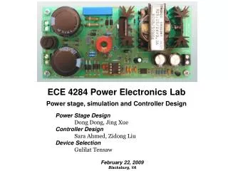
ECE 4284 Power Electronics LabPower stage, simulation and Controller Design Power Stage Design Dong Dong, Jing Xue Controller Design Sara Ahmed, Zidong Liu Device Selection Gulilat Tensaw February 22, 2009 Blacksburg, VA
Operation Spec. and Design Consideration Design Specification 1. Input voltage: 15~25V input 2. Output voltage: 5V, ripple 1% 3. Nominate output power: 25W 4. Half load change response: ΔVout within 5% 5. Primary side switching frequency 50 kHz 6. Controller phase margin 45o, gain margin 6dB • Consideration: • 1. Case Selection (input condition, output condition) • - Worst case for inductor and capacitor design • - Worst case for device selection • 2. Output capacitor ESR • - Capacitor design for voltage ripple suppression • - Controller design • 3. Flyback transformer design • - Physical design • 4. Controller design (RHP zero, resonant pole)
Operation waveform vC iM VC t t (1+D)T (1+D)T DT T DT T DC component of the Diode current goes to the load, and the rest goes to the Cap. iD ICo t (1+D)T DT T t (1+D)T T DT Io
Design Procedure Turn ratio selection Case selection Design L, C Duty cycle Check Duty cycle Calculate loss Check with control design Device Selection Finalize design
Duty Cycle & Turns Ratio The operation of converter can be divided into two topological modes: Modes 1 Modes 2 During D’T: During DT: &Dmax < 0.45 n = N2 : N1 = 2 : 3
Duty Cycle results • Assumptions: • R = 1 Ω • ESR of L: 15 mΩ • ESR of C: 10 mΩ • Rdson of MOSFET: 25 mΩ • VF of Diode: 0.65 V
Input Inductor & Output Capacitor Capacitor voltage: Inductor current: vC iM IM VC t t (1+D)T (1+D)T DT T DT T Worst case result: LM = 94.2 μH @ 25V C = 364.3 μF @ 15V
Impact of Capacitor ESR Vesr ICo vC t t (1+D)T (1+D)T T T DT DT Io VC Cap current ESR voltage t (1+D)T DT T VCo VC t DT T (1+D)T Ideal output voltage Real output voltage The existence of ESR increase the voltage ripple. If the ESR is too big, it can be the dominating factor to voltage ripple
Minimum Load Condition In order to verify the control performance at different load, the minimum load condition need to be found IL DT (1+D)T T t R = 6.667 Ω Minimum load: at the boundary of CCM & DCM
Device Requirement For device selection, the voltage and current stress need to be found Diode: Peak voltage: 21.55 V @ 25 V input Vdp t Average current: 5 A @ Nom. load (1+D)T DT T ID Switch: Peak voltage: 33.48 V @ 25 V input t (1+D)T DT T RMS current: 3.14 A @ 15 V input
Device selection Design Margin: Voltage Margin: 2:1 Current Margin: 1.5:1 Design Specs. for DIODE Design Specs. for MOSFET VRRM(repetitive peak reverse voltage of the diode) ≥ 43V IF(AV)(average forward current)≥ 13A VDS(rated drain to source voltage) ≥ 66V ID(rated drain current)≥ 8A Package: TO220 Package: SO8
Conduction loss and switching loss The MOSFET will experience both conduction and switching losses. Conduction loss: where Rds(on) = 150% (Rds(on) @ 25 oC) Switching loss: • The gate to drain “miller” charge, Qgd = 11nC; • Gate resistor, Rg= 1.2Ω; • Bias voltage, VDD = 40V; • Gate threshold of the MOSFET, Vgs(th) = 2V; • Output capacitance, Coss = 250pF Total loss: Ptot(loss) = Pcond+ Psw= 313mW
Thermal Design for MOSFET The selected MOSFET would have a junction to ambient thermal resistance of This thermal resistance is much more than the maximum Rth(ja) =80 k/C specified in the data sheet, and the junction temperature rise is just 50 k Heatsink is not required for the MOSFET
Loss and Thermal Design of Diode The switching loss of the Shcottky diode can be ignored where first term denotes the loss from forward rms current. second term denotes the loss from forward voltage conduction loss third term denotes the leakage current loss Thermal Design Rth(ja) = Rth(jc) + Rth(cs) + Rth(sa) where Rth(jc) = 1.6 k/w Rth(cs) = 1.8 k/w typical value of thermal resistance of Silicone thermal pad or Silicon thermal grease Rth(sa) = 19.2 k/w Heatsink for TO220 Package with 18.8 k/w is selected
Switching Model Open Loop Simulation in Saber • Simulation parameters: • Vin=15~25V • L=80µH, L_ESR = 15mΩ • C=680µF, C_ESR=7mΩ • Turns ratio : n1:n2=3:2 • fs=50kHz • Von=1V & Rdson=50mΩ • Maximum load R=1 Ω • Minimum load R=6.67Ω
Verification of Ripple Requirements with Simulations – Case 1: V=25V, R=1Ω • Maximum required voltage ripple =0.1V pk-pk (Vpk-pk=0.080397) • Maximum current ripple (20%) = 1.93796 pk-pk (Ipk-pk=1.6432)
Verification of Ripple Requirements with Simulations – Case 2: V=20V, R=1Ω • Maximum required voltage ripple =0.1V pk-pk (Vpk-pk=0.09101) • Maximum current ripple (20%) = 2.06316 pk-pk (Ipk-pk=1.4287)
Verification of Ripple Requirements with Simulations – Case 3: V=15V, R=1Ω • Maximum required voltage ripple =0.1V pk-pk (Vpk-pk=0.099323) • Maximum current ripple (20%) = 2.27636 pk-pk (Ipk-pk=1.3911)
Verification of Ripple Requirements with Simulations – Case 4: V=25V, R=6.67Ω • Maximum required voltage ripple =0.1V pk-pk (Vpk-pk=0.021112)
Verification of Ripple Requirements with Simulations – Case 5: V=15V, R=6.67Ω • Maximum required voltage ripple =0.1V pk-pk (Vpk-pk=0.021992)
Relationship between the output voltage ripple, capacitor value and ESR of the capacitor • Output voltage ripple is dominated by ESR in the output capacitor network. • Generally, the lower the ESR, the lower the output voltage ripple • Need a large capacitor to meet the step response Therefore, chose C=680µF with Resr=7mΩ (Part number: 565-3231-ND polyrad)
Implementing the Average Model in Simulink • The average model is derived as a buck-boost converter Power stage Controller • Applied step Power stage block
Controller Design • Steps followed: • Plot the open loop control to output voltage transfer function • Export the bode plot to sisotool and design a compensator that meets, • PM = 45 degrees and GM of 6dB • Export the compensator to the simulink model • Verify the transient response (Applying step) • Model the compensator transfer function with a real analog circuit (Opamp with R’s & C’s) • These steps (1-4) are repeated for all the following conditions: • Nominal input voltage (20V) with maximum load (R=1Ω) • Maximum voltage (25V) with maximum load (R=1Ω) • Maximum voltage (25V) with minimum load (R=6.67Ω) • Minimum voltage (15V) with maximum load (R=1Ω) • Minimum voltage (15V) with minimum load (R=6.67Ω)
Open loop control to output voltage transfer functions • Case with highest resonance (Q-point) • Maximum voltage (25V) and minimum load (R =6.67Ω) • Worst case for step response • Minimum voltage (15V) and maximum load (R= 1Ω)
Controller design • Key Points of Controller Design • Maximize low-frequency gain and minimize high frequency gain – An integrator is desired. • PID Controller which allows two zeroes to be added to raise slop upward and boost up to 180° phase. • The compensator is
Verifying the controller design for all cases to meet GM and PM
Verifying the controller design for all cases to meet GM and PM
Verifying the controller design for all cases to meet GM and PM
Verifying the controller design for all cases to meet GM and PM
Verifying the controller design for all cases to meet GM and PM
Transient response (Output current step from 2.5A-5A) – Minimum input voltage (15V)
Transient response (Output current step from 2.5A-5A) – Maximum input voltage (25V)
Extra credit part Transient response (Output current step from 0.1A-2.5A) – Maximum input voltage (25V) R=50 ohm to give I=0.1A
Transient response (Output current step from 0.1A-2.5A) – Minimum input voltage (15V) 35 "Hybrid AC/DC Power System Stability" - Weekly Meetings
Controller Realization as an Analog Circuit • The small signal model of the analog compensator is • Since our compensator transfer function is given as:
Controller Realization as an Analog Circuit • From the previous 2 equations:
Summary and Conclusions Design of the power stage and control circuit for a flyback dc/dc converter • Defined the specifications of the converter • Defined the converter operating point • Designed the passive components • Simulated the open loop switching and average model of the converter • Designed a compensator to meet the transient and step requirement • Selected some devices that would fulfill the loss and thermal design
Question? 39 "Hybrid AC/DC Power System Stability" - Weekly Meetings