X-ray Analysis in SEM: Identifying, Locating, and Quantifying Elements
200 likes | 318 Vues
Learn how to identify elements, locate the electron beam, acquire spectra, and perform detailed X-ray analysis in the SEM. Discover the 'what', 'where', and 'how much' of elemental analysis using ED and WD techniques.

X-ray Analysis in SEM: Identifying, Locating, and Quantifying Elements
E N D
Presentation Transcript
ED and WD X-ray Analysis Elemental analysis in the SEM The ‘what’, ‘where’ and ‘how much’?
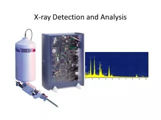
‘What’ - Identifying the elements Locate the electron beam on the region of the sample Start acquisition Spectrum shows peaks Elements are identified and labelled The higher the peak is above the background, the higher the concentration of that element
X-ray Generation L lines K lines
X-ray line series Sn L series Ca K series
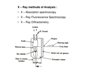
ED and/or WD? Energy dispersive Measures X-ray from its energy Wavelength dispersive Measures X-ray from its wavelength Energy in keV = 12.398/ wavelength in Angstroms
ED detectors Old type Si(Li) detectors needed to be kept at liquid nitrogen temperature New type SDD detectors are cooled to Peltier temperature X-ray energy converted to charge pulse and then to a voltage pulse Simultaneous acquisition of elements Be to U
WD spectrometer Diffraction according to Bragg’s law nλ=2dsinθ Much better peak resolution then ED Much better sensitivity for trace elements Sequential analysis of elements Be to U
ED and WD together resolution sensitivity
What can be analysed? Just about anything you can put in the SEM! Microanalysis – typical volume analysed about 1µm Depends on accelerating voltage and density Nanoanalysis – need to reduce electron beam penetration Reduce accelerating voltage For best results the sample should be flat and polished and conducting But often you can achieve adequate results from ‘rough’ samples
Typical applications Comparing ‘good’ and ‘bad’ samples Identifying compositions in fine grain structures Identifying sources of contamination Measuring variation in composition across an interface
Industrial and research applications Failure analysis - automotive, aerospace, semiconductors Materials research Quality Control Photovoltaics Light Emitting Diodes Thin film analysis Artefact conservation Steel inclusions Gun Shot Residue forensics
‘Where’ - Mapping Scan the electron beam and acquire X-ray information at each pixel position Display the results as a series of maps for each element or as a single colour image
Interaction volume Ni 5kV 0.1 µm 1µm Si 5kV 0.4 µm
Mapping large areas Field width 0.53mm3x3 maps stitched WD geometry requirement – will defocus at low mag.
Processing for quant Measure peak areas Compare with standards Apply inter-element corrections For accurate results, the sample should be flat, polished, homogeneous (on the micro-scale) and conducting
Detection limits Typically 0.1% to 0.5% for ED Order of magnitude better for WD Exact detection limit depends on operating conditions and composition
ED or WD? ED for major elements, fast analysis, rough samples Ideal for a ‘quick look’ WD for minor and trace elements and overlaps Better sensitivity and resolution, but slow ED and WD are complementary techniques for analysis