Source-gated Transistor
Source-gated Transistor. Seokmin Hong. Why do we need it?. * Short Channel Effects Source/Drain Charge Sharing Drain-Induced Barrier Lowering Subsurface Punchthrough Mobility Degradation Velocity Saturation And so on ….

Source-gated Transistor
E N D
Presentation Transcript
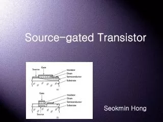
Source-gated Transistor Seokmin Hong
Why do we need it? * Short Channel Effects Source/Drain Charge Sharing Drain-Induced Barrier Lowering Subsurface Punchthrough Mobility Degradation Velocity Saturation And so on… No details, no explanation, only a kneeling of Intel's CEO and an excuse : We are in the transition towards a new architecture
Rectifying Contacts Forward bias Reverse bias
Conduction band minimum Vg=1V, Vd=0.2V Vg=0V, Vd=0.2V Vg=1V, Vd=0V C.-K. Huang, W.E. Zhang, and C.H. Yang, “Two-dimensional numerical simulation of Schottky barrier MOSFET with channel length to 10nm,” IEEE Trans. Electron Devices, vol. 45, pp842-848.1998.
* Source-gated structure • Small Saturation Voltage • (Saturation voltage coincides with • Vt(threthold voltage)) • High Output Resistance d & L=2um,Same semiconductor & insulation deposition
Transport Mechanism We constrict the flow of carriers using a source barrier and use the field effect to change the effective height of the barrier and the magnitude of the current. As the drain voltage is increased, the whole semiconductor region between the source and gate becomes depleted of charge. When this happens, the source current is determined by the voltage on the gate and is insensitive to further increase of voltage on the drain.
Basic Strategy Metal (Source) Metal (Gate) Oxide Semiconductor 1-D MOSFET Extraction of Band Bending Then we can get current using NEGF.
I-V relation between source and drain-(1) Relatively large leakage current when the transistor Is off. *Barrier Height = 0.2 V *Channel = 3 nm *Oxide thickness = 1 nm *Vg=0/0.25/0.5/0.75/1 V
I-V relation between source and drain-(1) *Barrier Height = 0.3 V *Channel = 3 nm *Oxide thickness = 1 nm *Vg=0/0.25/0.5/0.75/1 V
I-V relation between source and drain-(1) Reduced off-current *Barrier Height = 0.3 V *Channel = 6 nm *Oxide thickness = 2 nm *Vg=0/0.5/1/1.5/2 V
Source-gated transistor is fundamentally 2-D structureso it needs 2-D simulation!