Download

1 / 14
140 likes | 164 Vues
Explore the benefits of 2.5-D integration, assess interconnection characteristics, and develop physical design algorithms for high-performance systems. Comparison of 2-D and 2.5-D schemes. Improved timing, reduced power, and chip area.

E N D
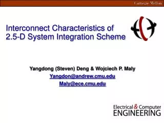
Interconnect Characteristics of 2.5-D System Integration Scheme Yangdong (Steven) Deng & Wojciech P. Maly Yangdon@andrew.cmu.edu Maly@ece.cmu.edu
Motivation • System-on-a-chip (monolithic integration) • Long wire delay dominates device delay • Mixed-technology design RISCcore Cache high performance logic DRAM PLL random logic Analog/RF System-on-a-Chip
2.5-D System Integration high performance logic analog/RF circuit stacked cache 2.5-D System CPU random logic DRAM • Technology and system co-design to achieve top performance • Potentials of 2.5-D System Integration • Allow optimum technology mix • Reduced chip area • Potential for top performance
Objective • Assess potential of 2.5-D system integration • Explore the solution space • Compare 2-D and 2.5-D integration schemes • Study the interconnection characteristics of 2.5-D Integration • Develop prototyping 2.5-D physical design algorithms • Formulation of problem • Implementation tradeoff
gate-level netlist block-level netlist 2-D floorplan 2.5-D floorplan 2-D placement 2.5-D placement placement approach floorplanning approach Approach • Coarse-grained approach – 2.5-D floorplanner • Fine-grained approach – 2.5-D standard cell placer • Conventional physical design tools for comparison
2.5-D System 2.5-D Via 2.5-D Interconnection • Different 2.5-D interconnection technologies are being developed • 2.5-D via is “expensive” • Fabricating cost • Consumed chip area • Optimizing wirelength using minimal number of 2.5-D vias
y y a a d d 0 Wa Wd T S 0 0 0 c c Wc b b 0 Wb x x BSG Based 2.5-D Floorplanner • Bounded Slice-line Grid (BSG)1 is a new floorplan representation • Maintain a BSG data structures for each die of 2.5-D system • Simulated annealing engine for optimization • New configuration: displacing, rotating, and swapping • Cost function: 1 S. Nakatate, et al., Module Placement on BSG-Structure and IC layout Applications, ICCAD, 1996
B19 Net 31 B3 B1 B32 B7 B8 B14 B30 B10 B17 B9 B19 B29 B25 B22 B14 B24 B18 B30 B7 B21 B10 B12 B15 B22 B5 B6 B23 B31 B29 B9 B8 B3 B20 2.5-D via B15 B28 B12 B5 B23 B11 B16 B18 B6 B17 B28 B24 B2 B0 B1 B11 B27 B32 B4 B13 B13 B26 B31 B26 B21 B27 B20 B16 B2 B0 B4 B25 Monolithic Floorplan 2.5-D Floorplan Floorplan of Benchmark Circuit AMI49
Results of Floorplanning • ami33 (33 modules, 123 nets) • ami49 (49 modules, 409 nets)
Min-Cut Bipartition 2.5-D Placer • Adapted from UCLA Capo placer • Netlist is first bi-partitioned by the multi-level partitioning engine • Iteratively place two sub-netlists
Wire Length • Average 16% total wire length reduction • Average 29% worst-case wire length reduction Design
Wire Length Distribution Number of Wires Scaled Local Nets Reduced Power Improved Timing micron
Conclusion • 2.5-D physical design tools • 2.5-D floorplanner and 2.5-D standard cell placer • 2.5-D integration scheme offers significant advantages • Reduced wire length • Improved timing and reduced power consumption • Reduced chip area
Subsequent Research • Industrial size designs to assess 2.5-D integration • Routability assessment of 2.5-D placement • Complete 2.5-D design flow • Refined 2.5-D physical design algorithms • Floorplan, placement, routing, … • Clock and power distribution in 2.5-D system • …