DEPFET development at the MPI Semiconductor Laboratory
400 likes | 652 Vues
DEPFET development at the MPI Semiconductor Laboratory. Gerhard Lutz MPI-Semiconductor Laboratory, München Vertex2003 Lake Windermere, Sept.16, 2003. Content. Introduction DEPFET detector-amplifier structure Principle and properties Applications DEFETs as pixel detector

DEPFET development at the MPI Semiconductor Laboratory
E N D
Presentation Transcript
DEPFET development at the MPI Semiconductor Laboratory Gerhard Lutz MPI-Semiconductor Laboratory, München Vertex2003 Lake Windermere, Sept.16, 2003
Content • Introduction • DEPFET detector-amplifier structure • Principle and properties • Applications • DEFETs as pixel detector • In x-ray astronomy (XEUS) • In particle colliders (TESLA) • DEPFET production in Munich • Vertex detector for TESLA • Detector thinning technology • Readout electronics • Summary and conclusions
Introduction • DEPFET detector development at Munich ispart of our activities in connection with instute experiments • Own laboratory is supported by two Max-Planck Institutes • Active in particle physics and astrophysics (X-ray astronomy) • Complete semiconductor processing line in house • Detectors mostly based on own concepts • Present major project: DEPFET pixel detectors
The Depleted Field Effect Transistor (DEPFET)Kemmer+Lutz 1985 • Device concept: • Combination of FET transistor with • Sideward depletion (Drift chamber)Gatti + Rehak 1984
DEPFET properties • Field effect transistor on top of fully depleted bulk • All charge generated in fully depleted bulk assembles underneath the transistor channel steers the transistor current • Combined function of sensor and amplifier • low capacitance and low noise • Signal charge remains undisturbed by readout ►repeated readout • Complete clearing of signal charge ►no reset noise • Full sensitivity over whole bulk • Thin radiation entrance window on backside DEPFET structure and device symbol
Operation modes of DEPFET • DEPFET operation properties • Charge collected and stored in internal gate bothin transistor on mode and alsoin transistor off mode • Charge is not destroyed by measuring it • DEPFET operation modes: • Normally on (continuous operation, occasional reset)►real time operation • Normally off (charge collection in powerless condition)►integration mode operation
Simulations operation modes • Real time mode: • Signal collection with DEPFET on • Real time signal processing (shaping) • Clear internal gate from time to time Applications: Readout element of drift detectors or CCDs Drain current Charge in internal gate Drain current
Simulations operation modes • Integration and Sample mode: • Signal collection with turned off DEPFET • Turn on DEPFET by gate • First current measurement • Clear internal gate • Remeasure current and take difference Applications: Building block of pixel detectors Readout element of drift detectors Drain current Charge in internal gate Drain current
DEPFET types: • MOS-depletion • MOS-enhancement • JFET • Open (rectangular) geometry • Closed (circular) geometry DEFET applications • Readout element of • Drift detector • CCD • Element of pixel detector
DEPFET 55Fe Spectrum • Single DEPFET • (JFET, closed geometry) • At room temperature • Cooled
MPI experiments needing DEPFETs • X-ray astronomy: • XEUS (next generationEuropean X-ray observatory)successor of XMM-Newton • Particle physics: • TESLA vertex detector • Both experiments need pixel detectors
DEPFET pixel matrix Low power consumption Fast random access to specific array regions • Read filled cells of a row • Clear the internal gates • of the row • Read empty cells • Difference of readings • (filled/empty) mesures charge
Prototype DEPFET-Systemdeveloped with Bonn University Control-Chip: Switcher 64x64 pixel DEPFET-Matrix JFET type Closed geometry (50x50µm2 pixel) low noise Readout-Chip: CARLOS • 64 x 64 matrix with 50 x 50 µm2 pixel • designed for Biomedical Applications • clock rate : 50 kHz • achieved noise in matrix: ~50e
Single-pixel spectra: 55Fe-spectra @ 300K ENC = 4.8 +/- 0.1 e- results with prototype system Matrix-picture with 55Fe: Autoradiography with 3H: ~ 3.2 mm ~ 10 mm detection of Tritium 3H (5,6keV mean energy) spatial resolution: ~ 9µm (with 50x50 µm2 pixel) [J.Ulrici, Bonn]
test & qualification simulation, layout & data analysis mounting & bonding MPI semiconductor laboratory 800 m² cleanroom up to class 1 ... ... with modern, custom made facilities ... ... for a full 6‘‘ silicon process line
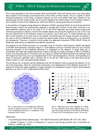
Future X-ray Mission: XEUS(X-ray Evolving Universe Spectroscopy) Scientific aim: investigation of the universe at an early evolution stage: - early black holes - evolution and clustering of galaxies - evolution of element synthesis • Experiment • Increase in collecting area (factor 100) • Increase of collection area (0.5 to 6-30m2) • Increase in focal length (7.5 to 50m) • Optics and focal imaging on separate satellites • Focal detector requirements: • faster readout (factor 10 to 100) • avoidance of ''out of time'' events • larger size focal detector (7x7cm2) • smaller pixel size (50•50μm2) • Detector requirements can be met with • DEPFET pixel detectors 6% “out of time” events in XMM
Present DEPFET pixel detector development forXEUS and TESLA In collaboration with Bonn (N.Wermes) and Mannheim (P.Fischer) TESLA vertex detector Thin Fast Low power Options: CCD MAPS HAPS DEPFET Total > 500 MPixel (with 25x25 µm Pixelsize) (read out speed 50 MHz)
Design of DEPFET pixel detectors • Type of DEPFETS: • MOS-depletion type • XEUS: zylindrical geometry • TESLA: rectangular geometry • Technology: • 6 Inch • Double-poly, • double metal, • Self-aligned
DEPMOS Technology Simulation • DEPMOS pixel array cuts through one cell Clear Gclear Channnel Metal 2 Metal 1 Oxyd Poly 2 Metal 2 Metal 1 Poly 2 Poly 1 p n+ Deep n Deep p Along the channel Perpendicular to the channel
Pixel prototype production (6“ wafer)for XEUS and LC (TESLA) Aim: Select design options for an optimized array operation (no charge loss, high gain, low noise, good clear operation) On base of these results => production of full size sensors Many test arrays - Circular and linear DEPFETS up to 128 x 128 pixels minimum pixel size about 30 x 30 µm² - variety of special test structures Structures requiring only one metalization layer Production up to first metal layer finished Devices are under test Test results agree very well with device simulations
First DEPFET measurements on rectangular test transistors (W = 120µm L = 5µm) Output characteristics: Correct transistor behavior Transfer characteristics: Device can be completely switched off Transistor parameters agree with simulation
Single circular DEPFET L = 5 µm, W = 40 µm time-continuous filter, τ = 6 µsec DEPFET test results: Noise and Spectroscopy
Rectangular double cell test structure • as used in TESLA pixel prototype
Single rectangular DEPFET: measure current with cleared internal gate As function of clear voltage Measure pedestal noise Compare situation of charge generation followed bysingle clear pulse with many clear pulses before reading DEPFET test resultsClearing of internal gate:complete clearing possible?At which voltage? Single clear pulse Many clear pulses
TESLA Module concept with DEPFETs • Sensor area thinned down to 50 µm • Remaining frame for mechanical stability • carrying readout and steering chips
readout chips steering chips reduce frame material!!! by etching of "holes" in the frame readout chips perforated frame: 0.05 % X0 total: 0.11 % X0 Module Concept 5-layer (CCD-like) layout for the vertex detector 1st layer module: sensitive area 100x13 mm2 sensitive area thinned down to 50 mm, supported by a directly bonded 300 mm thick frame of silicon Estimated Material Budget (1st layer): Pixel area: 100x13 mm2, 50 µm : 0.05% X0 steer. chips: 100x2 mm2, 50 µm : 0.008% X0 (massive) Frame :100x4 mm2, 300 µm : 0.09% X0
a) oxidation and back side implant of top wafer c) process passivation Top Wafer Handle <100> Wafer open backside passivation b) wafer bonding and grinding/polishing of top wafer d) anisotropic deep etching opens "windows" in handle wafer Processing thin detectors- the Idea -
Processing thin detectors - Direct Wafer Bonding - “SOI” Wafer prepared by MPI für Microstrukturphysik, Halle picture from: www.mpi-halle.mpg.de Q.-Y. Tong and U. Gösele “ Semiconductor Wafer Bonding ” John Wiley & Sons, Inc. picture from: www.mpi-halle.mpg.de
Direct Wafer Bonding possible, but some voids after annealing! improve surface condition before bonding Direct Wafer bonding after Implantation Bonded wafers (structured implant through BOX): infrared transmission pictures from MPI Halle (M. Reiche)
good selectivity to oxide almost perfect selectivity to Al no alkali ions poorer selectivity to (111) (≈30:1) rough surface after etching (hillocks) Anisotropic Wet Etching- TMAH - Tetra-Methyl-Ammonium-Hydroxide 54.72 deg
Type I: Simplified standard technology Type II: Implants like DEPFET config. p+ guard ring SiO2 SiO2 p+ Al Al n+ structured p+ on top unstructured n+ in bond region 3 Wafers unstructured n+ on top structured p+ in bond region 3 Wafers Diodes & Teststructures on thin Silicon * test bondability of implanted oxide & electrical performance of diodes on thin silicon * 2 types of thinned diodes n+ * + 4 Wafers with standard Diodes as a reference *
50 µm, standard diode, 10 mm2 250 µm, standard diode, 10 mm2 1/C2 (10-4 nF-2) 1/C2 (10-4 nF-2) bias voltage (V) bias voltage (V) C(Vfd) t = 46 mm Diodes & Teststructures on thin Silicon- Type I: CV curves, full depletion voltage -
250 µm, 4 standard diodes, 10 mm2 Diodes & Teststructures on thin Silicon- Type I: IV curves - 50 µm, 4 standard diodes, 10 mm2 back side completely free reverse current (pA) reverse current (pA) 800..950 pA/cm2 700..850 pA/cm2 bias voltage (V) bias voltage (V)
Diodes & Teststructures on thin Silicon- Type II: IV curves - Diodes of various sizes: 0.09 cm2 – 6.5 cm2 - no guard ring - - surface generated edge current included – reverse currents after annealing contact opening and metallization after etching of the handle wafer reverse current (nA) bias voltage (V) • about 2V full depletion voltage about 1 nA/cm2 including edge generated current
Readout electronics for DEPFET pixels • Developed in collaboration with other groups: • XEUS: MPE,Jülich,Buttler • TESLA: Bonn, Mannheim,MPI TESLA readout chip Current based readout Driver chips: Switching Clearing Row selection Readout chips: Signal amplification Pedestal subtraction Zero suppression
4.6 mm 4.8 mm New steering chipI.Peric (Bonn), P.Fischer (Mannheim) Switcher II: • AMS 0.8µm HV • versatile sequencing chip • (internal sequencer flexible pattern) • high speed + high voltage range (20V) • drives 64 DEPFET-rows • (can be daisy chained) • produced 12/2002 • Results: • power consumption: • ~1W /channel • tested ok to 30MHz
ISTORE I = I In + IBias I = I In + IBias Current based Readout How to store a current ?? Storage phase: input and sample-switch closed : gate-capacitance of nmoscharged Sampling phase:input and sample-switch opened : voltage at capacitance „unchanged“ current unchanged Transfer phase: output switch closed : (done immediately after sampling) ISTORE is flowing out
CURO - Architecture CURO : CUrrent Read Out • front end: automatic pedestal subtraction • (double correlated sampling) • - easy with currents - • analog currents buffered in FIFO • Hit-Logic performs 0 suppression • and multiplexes hits to ADC • (ADC only digitizes hits !)
Results - CURO I (Marcel Trimpl, Bonn) CURO I: • TSMC 0.25µm, 5metal • contains all blocks for a fast DEPFET R/O • radiation tolerant layout rules with annular nmos • produced 05/2002 1.5 mm digital part: works with desired speed (50MHz) 4 mm • analog part (current memory cell): • tested up to: 25MHz • differential non-linearity: 0.1 % • noise contribution to readout: < 39nA Crucial parts of readout work Design of CURO II submitted Delivery Dec.03 TESLA Goal: Thin fullsize pixel matrix 2005
Summary • DEPFET structure invented 1984 • Offers many unique features and applications • Development in MPI Semiconductor Detector Laboratory • with high-tech production technology • in collaboration with other institutes • DEPFET pixel detectors for • X-ray astronomy (XEUS) • Particle physics (TESLA) • are major projects of the laboratory • Other applications are also foreseen • Development is progressing very well