Outline Semiconductor equations Examples pnCCD Depleted Field Effect Transistor (DEPFET)
290 likes | 518 Vues
Semiconductor device simulation of silicon radiation detectors R. H. Richter for the MPI Semiconductor Lab. Outline Semiconductor equations Examples pnCCD Depleted Field Effect Transistor (DEPFET) Pixel detectors: field distribution in heavily irradiated silicon Summary.

Outline Semiconductor equations Examples pnCCD Depleted Field Effect Transistor (DEPFET)
E N D
Presentation Transcript
Semiconductor device simulation of silicon radiation detectorsR. H. Richter for the MPI Semiconductor Lab Outline Semiconductor equations Examples pnCCD Depleted Field Effect Transistor (DEPFET) Pixel detectors: field distribution in heavily irradiated silicon Summary
Continuity equations Equations • Simultaneous consideration of • Generation • Recombination • Drift • Diffusion • Drift due to electric field derived from Poisson Equation • Numerical simulation: simultaneous solution of diffusion and Poisson equation with boundary conditions R. H. Richter, 6th Hiroshima Symposium - STD6, Carmel, September 12th 2006
Boundary conditions and features • Neumann b.c. (termination and symmetric continuation) • Direchlet b.c. (Ohmic contacts) • Gate b.c. • Schottky contacts • Simple networks with R,C,L possible • Sophisticated mobility models • Parametrization of impact ionization (avalanche) R. H. Richter, 6th Hiroshima Symposium - STD6, Carmel, September 12th 2006
Concept of PN-CCD with frame store(Google-> pnCCD, XMM) PN-CCD different from MOS-CCDs anode + JFET on chip per channel pn-junctions instead of MOS gates p n p transfer “deep” in bulk fully depleted 0.5 mm pn-junction (homogeneous) backside illumination R. H. Richter, 6th Hiroshima Symposium - STD6, Carmel, September 12th 2006
pnCCD – simulation tasks • WIAS-TeSCA • 2D-Simulation • charge transfer • barriers to surface • Transfer region + anode • charge transfer to anode • Channel separation (perpendicular to transfer region) • Technology compatibility with on chip amplifiers (JFETs). • Challenges: large domain (50000 triangles), depletion state - electrons • How to verify? R. H. Richter, 6th Hiroshima Symposium - STD6, Carmel, September 12th 2006
Meshing • Triangulated grid (2D) often taken from the • technolgy simulator but additional programs • are also used (Gridgen, B. Heinemann) 20.000 – 40.000 points R. H. Richter, 6th Hiroshima Symposium - STD6, Carmel, September 12th 2006
potential log(n) Localized generation of e/h pairs simulate particle tracks or converted photons.
pn-CCD performance • largest monolithic CCD • 6 x 6 cm² • 384 x 400 pixel • 150 µm pixel • fast, parallel readout • 5 msec full frame • low noise • 4 el. rms • high quantum efficiency • 90 % • radiation hard • 400 Mp/cm²
XMM-Newton – first light (January 2000) large Magellanic cloud supernova remnant 1987A
Getting insight into a CCD - Mesh Analysis of the charge collection process Mesh experiment (Tsunemi, Yoshita, Kitamoto, Jpn J. Appl. Physics 36, 2906 N. Kimmel et al, Analysis of the charge collection process in pnCCDs , Proceedings of SPIE vol. 6276, p. R. H. Richter, 6th Hiroshima Symposium - STD6, Carmel, September 12th 2006
Mesh-results vs Simulation Charge distribution over the pixel Simulation: charge generation in steps of 5µm scanning the transfer direction R. H. Richter, 6th Hiroshima Symposium - STD6, Carmel, September 12th 2006
CTE degradation due to traps • You can’t predict the real life completely. Even if you create ‘perfect’ transfer potential with a lot of headroom. • N. Krause et al, NIM A439, p228 • Contamination in epitaxial layers (gas delivery, stainless steel) • Titanium contamination (ET about 0.26eV, several 1010cm-3) during epitaxy (also measured with DLTS) • Replace the epitaxial layer High energy implantation (P 20MeV) R. H. Richter, 6th Hiroshima Symposium - STD6, Carmel, September 12th 2006
pn-CCD – charge transfer efficency Replacing the epitaxial layer by a 20MeV HE P-impl. R. H. Richter, 6th Hiroshima Symposium - STD6, Carmel, September 12th 2006
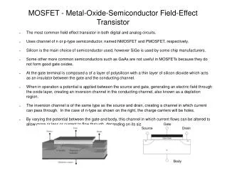
DEPFET-Principle of Operation MIP source top gate drain clear bulk n+ p+ p+ n+ n+ p n s i internal gate x a + - - y - - - r t - - e + m - m y s + - n + - p+ rear contact Potential distribution: internal Gate ~1µm Backcontact Drain 50 µm Source [TeSCA-Simulation] FET-Transistor integrated in every pixel (first amplification) Electrons are collected in „internal gate“ and modulate the transistor-current Signal charge removed via clear contact R. H. Richter, 6th Hiroshima Symposium - STD6, Carmel, September 12th 2006
DEPFET-Principle of Operation +15V source top gate drain clear bulk 0V 0V n+ p+ p+ n+ n+ p n s i internal gate x a - - y - - - r t - e m m y s - n p+ rear contact Potential distribution: internal Gate ~1µm Backcontact Drain 50 µm Source [TeSCA-Simulation] FET-Transistor integrated in every pixel (first amplification) Electrons are collected in „internal gate“ and modulate the transistor-current Signal charge removed via clear contact R. H. Richter, 6th Hiroshima Symposium - STD6, Carmel, September 12th 2006
DEPMOS Technology on high ohmic 6” wafer(DIOS-ISETCAD-Simulation) • DEPMOS pixel array cuts through one cell Clear Gclear Channnel Metal 2 Metal 1 Oxyd Poly 2 Metal 2 Metal 1 Poly 2 Poly 1 p n+ Deep n Deep p Along the channel Perpendicular to the channel Double poly / double aluminum process on high ohmic n- substrate Low leakage current level: < 200pA/cm² (fully depleted – 450µm) R. H. Richter, 6th Hiroshima Symposium - STD6, Carmel, September 12th 2006
Potential of the empty Internal Gate L = 4 (3) µm L= 5 (4) µm L = 6 (5) µm L = 7 (6) µm L = 10 (9) µm ToSCA – 2D device simulation R. H. Richter, 6th Hiroshima Symposium - STD6, Carmel, September 12th 2006
Comparison with simulation – internal amplification vs channel length • Simulation @ 50µA drain current • Assuming an under-etching of 1.2µm • Measured by S. Rummel measured at 100µA measured at 50µA nice illustration of the DEPFET scaling potential R. H. Richter, 6th Hiroshima Symposium - STD6, Carmel, September 12th 2006
DEPFET 3D-Simulation K. Gärtner, R.R., DEPFET sensor design using an experimental 3d device simulator, accepted for publication in NIM ILC layout R. H. Richter, 6th Hiroshima Symposium - STD6, Carmel, September 12th 2006
Simulated signal response Introduction of: buried channel implantation lateral drift fields by inclined deep p implantations Charge reaches the interface -> slow diffusion In reality: charge loss due to trapping and small potential barriers R. H. Richter, 6th Hiroshima Symposium - STD6, Carmel, September 12th 2006
Bias Bias Bias Gate #1 Gate #2 Gate #1 Gate #1 Gate #2 Gate #2 Auslese- knoten #1 Clear #1 Clear #2 Auslese- knoten #2 Auslese- knoten #1 Auslese- knoten #1 Clear #1 Clear #1 Clear #2 Clear #2 Auslese- knoten #2 Auslese- knoten #2 Transfer- gate Transfer- gate Transfer- gate Bias Gate #1 Gate #2 Bias Bias Gate #1 Gate #1 Gate #2 Gate #2 Auslese- knoten #1 Clear #1 Clear #2 Auslese- knoten #2 Transfer- gate Auslese- knoten #1 Auslese- knoten #1 Clear #1 Clear #1 Clear #2 Clear #2 Auslese- knoten #2 Auslese- knoten #2 Transfer- gate Transfer- gate RNDR principle(repetitive non destructive readout ) • By measuring the charge multiple (n) time the noise can be reduced by 1/ sqrt(n) • Because the collected charge is stored during readout in the DEPFET-RNDR, the very same charge can be measured multiple times. R. H. Richter, 6th Hiroshima Symposium - STD6, Carmel, September 12th 2006
Investigated Structure: 4x4 Minimatrix(G. Lutz) • ILC-Type RNDR • Realised as a four by four Minimatrix R. H. Richter, 6th Hiroshima Symposium - STD6, Carmel, September 12th 2006
Laser spectra (S. Wölfel) • Measurement: • Charge injection with laser during integration time • 180 Loops for the readout (duration: 9.18 ms) -45 °C • Measured leakage current: • ca. 0,4 e- in 180 loops Noise Limit 0,25 e- R. H. Richter, 6th Hiroshima Symposium - STD6, Carmel, September 12th 2006
Double trap model for heavily irradiated silicon • V. Chiocia et al (accepted for Proceedings of Wildbad Kreuth (NIM A)) see also Eremin, Verbitskaja, Li, NIM A476, p.556 R. H. Richter, 6th Hiroshima Symposium - STD6, Carmel, September 12th 2006
Charge collection profile by grazing angle techniqueon a CMS pixel detector (testbeam measurement) R. H. Richter, 6th Hiroshima Symposium - STD6, Carmel, September 12th 2006
Simulated and measured charge 10V 15V 20V 0.5 x 10¹⁴ neq 2 x 10¹⁴ neq 25V 150V 50V 100V R. H. Richter, 6th Hiroshima Symposium - STD6, Carmel, September 12th 2006
Electric fields 0.5 x 10¹⁴ neq 2 x 10¹⁴ neq unirradiated R. H. Richter, 6th Hiroshima Symposium - STD6, Carmel, September 12th 2006
Summary • Developing state of the art detectors there is no way around a thorough • numerical simulation. • Primary task: Prediction of the device behavior and finding optimal operation states and process parameters • Provides insight into the potential and limits of a device concept. • For a full understanding of complicated pixel detectors 3D-simulation is a must! • Investigation of radiation induced defects by the ‘grazing angle technique’ together with simulations is a promising way. R. H. Richter, 6th Hiroshima Symposium - STD6, Carmel, September 12th 2006