Download
1 / 30
300 likes | 319 Vues
MPE Max-Planck Institut für extraterrestrische Physik. WHI Max-Planck Institut für Physik (Werner-Heisenberg-Institut). PNSensor GmbH. Development of backside illuminated Silicon Photomultipliers at the MPI Semiconductor Laboratory. Outline:

E N D
MPE Max-Planck Institut für extraterrestrische Physik WHI Max-Planck Institut für Physik (Werner-Heisenberg-Institut) PNSensor GmbH Development of backside illuminated Silicon Photomultipliers at the MPI Semiconductor Laboratory • Outline: • Motivation for a backside illuminated SiPM (BID-SiPM) • Layout of BID-SiPM • R&D Program • Results and Simulations (preliminary) • Applications in Particle Physics • on behalf of the MPI SiPM group
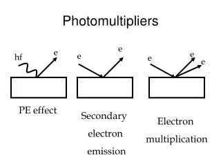
Motivation for backside illumination In general SiPM offer great advantages compared to photomultiplier tubes: Simple, robust device Photon counting capability Easy calibration (counting) Insensitive to magnetic fields Fast response (< 1 ns) Large signal (only simple amplifier needed) competitive quantum efficiency (~ 40% at 400-800 nm) No damage by accidental light Cheap Low operation voltage (40 – 70 V) R&D goal: Increase Quantum efficiency to the physical limit
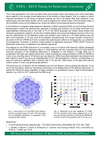
QE & Fill Factor • What limits the QE? • QE = surface transmission • x Geiger efficiency • x geometrical fill factor • Front illuminated devices: • Large area blinded by structures • Al-contacts • Bias-resistor • Guard rings/Gap between HF implants • For 42 x 42 mm2 device: 15% fill factor • Solutions: • larger pixel size (80% reached for 100 mm pitch device) • back-illumination light enters through homogeneous back side, not covered by any structure 3 mm light spot scanned across device
Geiger Efficiency of electrons and holes Electrons have a higher probability to trigger an avalanche breakdown then holes Efficiency depends on depth of photon conversion and hence on the wavelength • Solutions: • Increase overvoltage • Or: • - Ensure that only electrons trigger an avalanche n+ p+ holes el. p+ n+ el. p- epi n- epi holes p-substrate n-substrate
Electrons trigger avalanche Holes trigger avalanche Thin entrance window needed holes electrons Sensitivity at different wavelengths Example: p-substrate p-substrate: photons < 450 nm: only holes contribute photons > 700 nm: lost in insensitive bulk n-substrate: ok for short wavelengths, hole efficiency dominates for l > 500 nm Back illumination: whole thick (> 50 mm) bulk absorbs photons design for electron collection
Concept of a back illuminated SiPM Combine SiPM and drift (photo) diode: Each Pixel of a SiPM array is drift diode with a geiger APD as amplifying element in the center By drift rings the electrons from photon conversions are focused into a small HF region Homogeneous sensitivity, no dead regions Back Illuminated Drift SiPM BID-SiPM g
Design of the avalanche cell The HF region is created between a n+ contact at the surface and a deep p well underneath. By modulating the depth of the p-implant and/or the n-contact the HF region can be confined to a small area of a few mm diameter -> Small HF region: Low capacitance, low gain (important to fight cross talk)
Engineering of Entrance Window Homogeneous, unprocessed thin entrance window at backside - minimal UV absorption in surface layer (important for l < 350 nm) - possibility of antireflective coating (Calculation: R. Hartmann)
Disadvantages • Large volume for thermal generated currents (increased dark rate) Maintain low leakage currents Cooling Thinning ( < 50 mm instead of 450 mm) • Large volume for internal photon conversion (increases x-talk) Lower gain (small diode capacitance helps) Possible show stopper! • Electron drift increases time jitter Small pixels, Increased mobility at low temperature <2 ns possible
Design of Devices Hexagonal Cells 100-200 mm diameter Up to 3 three drift rings Central HF region with <8 mm diameter Capacitance ~ 5 fF Gain: O(105) ~ 1 mm depth 95% Geiger efficiency @ 8V overvoltage (electrons) Drift field extends into bulk
Test structure production in 2005 -> fix parameters of avalanche cell (radius, depth, resistor values…) -> no backside illumination yet Single pixel structures Small arrays Large arrays (20 x 25 pixel 180 mm pitch) HF diameter: 5-25 mm Successfully tested
Results: Test Structures Low Medium High Results with light pulses from a laser (< 1 ns): Photoelectron peaks clearly resolved up to large n(photon) RMS of single photoelectron signal ~ 5%
Results: Test Structures T = 0oC T = 10oC T = 20oC Gain proportional to overvoltage Breakdown voltage in good agreement with device simulations
Test Structures Dark rate mainly from highly doped HF region: For a 5 x 5 mm2 matrix with 500 pixels: ~0.2 MHz @ 20oC(8V)
Leakage Currents and Dark Rates Back side illuminated: bulk leakage current dominates: For devices thinned to 50 mm: ~10MHz @ 20oC Cooling needed: ~ 1 MHz @ 0oC
Processing thin detectors (50 mm) a) oxidation and back side implant of top wafer c) process passivation Top Wafer open backside passivation b) wafer bonding and grinding/polishing of top wafer d) deep etching opens "windows" in handle wafer Successfully tested with MOS diodes (keep low leakage current ~ 100 pA/cm2)
Cross Talk Studies entries Dark spectrum of 25 mm arrays x-talk heavily suppressed due to small HF region and large pitch Background due to pile up (suppressed by cooling to -20 C) 2pe signal clearly visible: Probability for x-talk ~ 10-4 (@*V DU) For backside illumination: Bulk is sensitive to cross-talk photons Use MC to extrapolated to full structure 1 pe ~ 2x10⁶ 2 pe < 200 V
drift drift e e Monte Carlo Simulation of cross talk Generate photons Propagate through device • Photon Converts • In pixel of origin • In neighbour pixels • Active region • Apply geiger efficiency
Monte Carlo Simulation of cross talk Generate photons Number of photons poisson distributed Lacaita, IEEE TED, 40 (1993): 2.9 photons/105 e- (E > 1.14 eV) Propagate through device Use black body spectrum with T=4300K -However: el/holes not in thermal equilibrium -Band structure not taken into account (2.9 ph > 1.14 eV => 8.5 ph total) • Photon Converts • In pixel of origin • In neighbour pixels • Active region • Apply geiger efficiency
e e Monte Carlo Simulation of cross talk 1 mm Generate photons 100 mm Propagate through device Calculate photon absorption length From Photon energy • Photon Converts • In pixel of origin • In neighbour pixels • Active region • Apply geiger efficiency Surface reflection given by n=3.57
drift drift Monte Carlo Simulation of cross talk Generate photons Propagate through device • Photon Converts • In pixel of origin • In neighbour pixels • Active region • Apply geiger efficiency Electrons: drift in HF region (if bulk depleted) Apply local Geiger efficiency (as function of overvoltage)
Monte Carlo Simulation of cross talk Generate photons Propagate through device • Photon Converts • In pixel of origin • In neighbour pixels • Active region • Apply geiger efficiency Cross talk spectrum
Cross talk spectrum Contribution from photons with range from O(pitch) – O(mm)
Dependence on Pitch larger pitch -> x-talk spectrum narrow Larger pitch -> less x-talk
Results Cross talk measured with test structures implies: ~54 photons (E>1.14 eV) per avalanche (@*V DU) For a backside illuminated device with 100 mm pitch: cross-talk probability: 99.99% Due to large capacitance (47 fF of HF region + coupling capacitances), the gain is very high: ~4 x 10⁶ Scaling to the expected gain of 105: Cross talk 20-30 % Still high but could be manageable Extrapolation has large systematic error!
Further Program 2nd step: production of fully functional backside illuminated SiPMs: -> including drift rings -> double sided processing, deplete bulk Finished: End 2007 Various test structures (single pixel, small arrays) Arrays: 30 x 31 pixel Diameter HF region: < 8 mm Pitch: 100, 120, 150, 200 mm Area: 3x3 mm2 – 6x6 mm2 In addition: some front illuminated arrays
Applications in (Astro-) Particle Physics • Main advantages: Drawbacks: • High QE Dark rate • Good sensitivity for Cross talk • 300nm < l < 1000nm Costs • (double sided processing) • Can be used where QE and spectral response are important but high dark rate can be tolerated • Air cerenkov telescopes - peak wavelength 300-350 nm • (like MAGIC) - considerable LONS background
Applications • Cerenkov detectors in particle physics detectors • Compact high density calorimeters low light yield, direct coupling to blue scintillator • In colliding beam experiments: dark rate can be suppressed using coincidence with beam no self trigger needed (cross talk!) • Large scale applications (big calorimeters) probably excluded (costs) Practical advantage: Direct coupling of entrance window to scintillator (no wire bonds) Scintillator SiPM Readout board
SiPM BiCMOS analogue clock x, y, t CMOS digital Smart SiPMs • Connect ASIC chip to back-illuminated SIPM • For each pixel: signal detection & active quenching • Fast timing (no stray capacitances) • Low threshold -> low gain • Active quenching -> low gain • Minimal cross-talk • Single pixel position resolution • Veto of noisy pixels g • Could be made using • Bump bonding • 3D integration techniques
Summary Backside illuminated Silicon Photomultipliers are developed at the MPI Semiconductor Laboratory Application: Upgrade of Magic Camera Aim for highest quantum efficiency in a large spectral range (only limited be quality of entrance window) First test structures (not yet back illuminated) produced and tested Production of full devices ongoing Design goals: QE: 80% for 300 – 950 nm, peaking at > 90% Dark rate: <1MHz for 0.25 cm2 device @ 0oC Gain: 105 Cross talk: 20-30 % ? High cross talk is of major concern!