Download
1 / 10
100 likes | 412 Vues
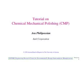
Development of Chemical-Mechanical Polishing for Superconducting Cavities. Shekhar Mishra, Fermilab Mark J. Oreglia, Univ. of Chicago Cliff Spiro, Cabot Microelectronics. Project Summary. High Gradient (~35 MV/m) and high yield of the SRF cavities are needed for

E N D
Development of Chemical-Mechanical Polishing for Superconducting Cavities Shekhar Mishra, Fermilab Mark J. Oreglia, Univ. of Chicago Cliff Spiro, Cabot Microelectronics
Project Summary • High Gradient (~35 MV/m) and high yield of the SRF cavities are needed for • International Linear Collider (ILC) and High Intensity Proton Accelerator (Project-X). • State of the art cavity manufacturing and processing : • Electo-polishing and High Pressure Rinse • Remove the damaged Niobium layer • Average Gradient is 20% lower • Yield is less than 25% • Limitation: • Complicated procedure, dangerous chemical, expensive • Niobium surface contamination and/or surface imperfection caused by either manufacturing or processing (Sulfur contamination) • Proposal: • Chemical-Mechanical Planarization technology to remove the damaged Niobium layer ANL-FNAL-UofC Collaboration Meeting
9-cell Test Results ILC Goal Average A6-8, AES2,4 = 32 MV/m A9 reprocess at Jlab ANL-FNAL-UofC Collaboration Meeting
Why alternate technique ? • The electrolyte is a mixture of hydrofluoric and sulfuric acid. Details not fully understood. • Manufacturing or acid related defect: ~600µm beads on Nb cavity • Acid related contamination • Sulfur Deposit • Surface Smoothness: RMS: • 1247 nm fine grain BCP • 27 nm single crystal BCP • 251 nm fine grain ep z θ These two problems will require mechanical polishing that can make a smooth surface. 1mm ANL-FNAL-UofC Collaboration Meeting
Introduction to Cabot Microlectronics and Chemical Mechanical Planarization (CMP) • Leader in CMP slurries • Pioneer in CMP technology • Copper, Tungsten, Dielectric, Data Storage • CMP pad offering in early stage commercialization • ESF consumable and service offering in non-semiconductor applications • Unparalleled track record • Deliver tens of millions of gallons to customers globally • Outstanding technology and manufacturing infrastructure • Robust ramp of new products to high volume production • Provide global support and service • World-class team of scientists and technologists Non-planarized IC product PlanarizedIC product
CMP of Nb 20X Field of View (approx. 230um x 300um) BEFORE Rq = 603nm Heavily cratered surface from machining AFTER Rq = 3.5nm Small islands appear to be grains. Highest point to lowest point around 18.6nm.
Fermilab Tumbling Machine Not installed. Design and Engineering needed to hold the cavity in place and liquid flow etc. ANL-FNAL-UofC Collaboration Meeting
New Vertical Test @ FNAL Nine-cell Tesla-style cavity • Recently commissioned (IB1) • Existing 125W@ 1.8 K Cryogenic plant • RF system in collaboration with Jlab • Capable of testing ~50 Cavities/yr • Evolutionary upgrades: • Thermometry for 9-cells, 2 cavities at a time, 2 top plates, Cryo upgrades • Plan for two additional VTS cryostats • Ultimate capacity ~ 264 cavity tests/yr Plan for 2 more VTS pits VTS Cryostat:IB1 New RF & Control Room ANL-FNAL-UofC Collaboration Meeting
Plans and Possibilities • Development of the chemical that would be used in the Chemical Mechanical Polishing (CMP) of Niobium • Small sample test • Accelerating Gradient Test: • Polish 1-cell (1.3 GHz) Nb cavity using the Fermilab Tumbling machine • Rinse with high purity water • RF test in the Fermilab Vertical Test Facility • Possible Advantage • No dangerous chemical • A much simplified procedure that could lead to considerable cost saving • Could potentially reduce acid related defects and contamination • Could eliminate surface defects produced during manufacturing • Small size R&D project with great potential • Excellent training opportunities for students in Accelerator R&D ANL-FNAL-UofC Collaboration Meeting
Budget • Build on Surface science Research • Student training in Accelerator R&D (Fermilab Accelerator Ph.d Program) • Local Industry involvement • Leverage existing laboratory infrastructure ANL-FNAL-UofC Collaboration Meeting