Download

1 / 28
410 likes | 924 Vues
8086 Bus Design. Khaled A. Al- Utaibi alutaibi@uoh.edu.sa. Agenda. Buffering and Latching 8086 Bus System Bus Timing Bus Write Cycle Read Cycle Ready and Wait States 8086 Bus System Design Objective Requirements Procedure. Buffering and Latching.

E N D
8086 Bus Design Khaled A. Al-Utaibi alutaibi@uoh.edu.sa
Agenda • Buffering and Latching • 8086 Bus System • Bus Timing • Bus Write Cycle • Read Cycle • Ready and Wait States • 8086 Bus System Design • Objective • Requirements • Procedure
Buffering and Latching • Before starting with 8086 bus system design, one needs to understand the following concepts: • (1) Fan-out limitations of logic gates • (2) Buffering • (3) Latching
Buffering and Latching Fan-out Limitations • If the output of some gate A isconnected to the input of another gate B, gate A is said to be driving gate,while gate B is said to be the load gate. • The fan-out of a gate is the largest number of gate inputs this gate can drive. • The fan-out for TTL is 10loads. • The fan-out for CMOS is 8 loads A B Driver Gate Load Gate
Buffering and Latching High-Drive Buffers • A buffer is a single input single output gate that provides the necessary drive capability which allows driving larger loads.
Buffering and Latching Tri-State Buffer • The outputs of 2 logic gates can not be directly connected because this causes a short circuit that results in huge current flow may result in damaging the circuit • The solution to this problem is to use tri-state buffers. • A tri-state buffer is a special gate with 3 states controlled by an enable input (E) : • Logic 0 (Low Voltage), • Logic 1 (High Voltage), and • Hi-Impedance(Open Circuit)
Buffering and Latching Bidirectional Buffers • 74LS245 3-State Bidirectional Octal Buffers:
Buffering and Latching Unidirectional Buffers • 74LS244 3-State Unidirectional Octal Buffers:
Buffering and Latching Simple D-Latch • The D-Latch is a memory device which can store one bit of data for as long as the device is powered. • The D-Latch has one data input (D), one control input (C) and one data output (Q/Q’). • When C = 0, the output Q keeps its value (No Change) • When C = 1, the output Q follows the input D (Q = D)
Buffering and Latching D-Latches with Tri-State Buffers • 74LS374 3-State Octal D-Type Transparent Latches :
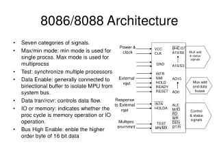
8086 Bus System • The 8086 has three buses • (1) Address Bus: provides memory and I/O with the memory address or the I/O port number • (2) Data Bus: transfers data between the microprocessor and the memory and I/O • (3) Control Bus: provides control signals to the memory
8086 Bus Timing • 8086 access memory and I/O devices in periods called bus cycles. • Each cycle equals 4 system-clocking periods (T states). • If the clock is operated at 5 MHz, one 8086 bus cycle is complete in 800 ns.
8086 Ready and Wait States • The READY input causes wait states for slower memory and I/O components. • A wait state (Tw) is an extra clocking period inserted between T2 and T3. • The READY input is sampled (checked) at the end of T2 and in the middle of Tw. • If READY is a logic 0 at the end of T2, then T3 is delayed and Tw is inserted between T2 and T3 • READY is next sampled at the middle of Tw to determine if the next state is Tw or T3. • The READY signal is synchronized with clock using the 8284A clock generator.
8086 Bus System Design Objective • Objective: to provide the system the three main buses required to access memory and I/O devices • (1) Address Bus • (2) Data Bus • (3) Control Bus
8086 Bus System Design Requirements • Requirements: bus design must satisfy two main requirements • (1) Bus Buffering:the system must be buffered if the number of devices interfaced to it is more than its fan-out • (2) Bus Demultiplexing (Latching):All time multiplexed lines of the processor must be first demultiplexed (latched) to split address, data, status and control lines before interfacing them to memory and I/O devices.
8086 Bus System Design Procedure • Designing a bus system involves the following steps: • (1) Identify input, output and input/output pins of the processor. Note that only output and input/output pins are considered for designing the bus system (i.e. input pins are not part of the bus system). • (2) Identify time multiplexed pins of the processor. These pins need to be demultiplexed. • (3) Use latches to demultiplex time multiplexed pins. • (4) Use buffers to buffer all data, address and control lines to be connected to memory and I/O devices. • Latched lines are already buffered. • Input/output lines require bidirectional buffers • Output lines require unidirectional buffers
8086 Bus System Design ProcedureExample • Design a fully buffered and de-multiplexed bus system for a minimum mode 8086-based microcomputer system.
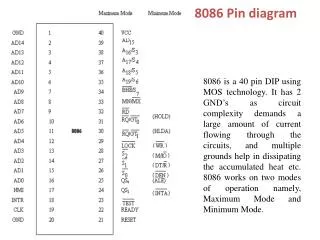
8086 Bus System Design Procedure(1) Identify Inputs, Inputs/Outputs & Outputs • Inputs: these are not part of bus system design • VCC • GND • NMI • INTR • CLK • RESET • READY • TEST’ • HOLD • MN/MX’
8086 Bus System Design Procedure (1) Identify Inputs, Inputs/Outputs & Outputs • Outputs: • A16/S3 • A17/S4 • A18/S5 • A19/S6 • RD’ • HOLDA (not required, why?) • WR’ • M/IO’ • DT/R’ • DEN’ • ALE • INTA’ (not required, why?)
8086 Bus System Design Procedure (1) Identify Inputs, Inputs/Outputs & Outputs • Inputs/Output: • AD0-AD15
8086 Bus System Design Procedure (2) Identify Time Multiplexed Pins • Time Multiplexed Pins: • AD0-AD15 • A16/S3-A19/S6 • BHE’/S7
8086 Bus System Design Procedure (3) Latching (Demultiplexing) Multiplexed Lines • As shown in Step(2), the 8086 has 21 multiplexed lines: • AD0-AD15 • A16/S3-A19/S6 • BHE’/S7 • To latch (demultiplex) these lines using 74LS373 octal latches, we need 21/8 = 3 chips. • The input controls of the 74LS373 octal latches should be connected as follows : • Output Control (OE’) connected to GND (Why?) • Latch Enable (G’) connected to ALE (Why?)
8086 Bus System Design Procedure (4) Buffering Address, Data & Control Lines • The data lines D15-D0 should buffered using bidirectional buffers (74LS245). Why? • We have 16 data lines. So, we need 16/8 = 2 chips. • The Buffer Enable (G’) should be connected to DEN’ (Why?) • The Direction Control (DIR) should be connected to DT/R’ (Why?) • The Control Lines M/IO’, RD’ and WR’ should be buffered using unidirectional buffers (74LS244). Why? • The Buffer Enable (G’) should be connected to GND (Why?)
8086 Bus System Design Procedure (4) Buffering Address, Data & Control Lines • Since address lines A19-A0 & BHE’ are latched using 74LS373 octal latches, they are already buffered. • The following control lines are will not be buffered: • DT/R’ & DEN’ because they are will not be connected to memory or I/O devices. • HOLDA because the direct memory access is not supported by our system. • INTA’ because interrupts are not supported by our system.

![8086 [2]](https://cdn1.slideserve.com/2457127/8086-2-dt.jpg)