Download

1 / 65
690 likes | 1.11k Vues
8086 and families. Features of 8086. 16Bit Microprocessor : 8086 - 8086 is a 16bit processor. It’s ALU, internal registers works with 16bit binary word - 8086 has a 16bit data bus. It can read or write data to a memory/port either 16bits or 8 bit at a time

E N D
Features of 8086 • 16Bit Microprocessor : 8086 • - 8086 is a 16bit processor. It’s ALU, internal registers works with 16bit binary word • - 8086 has a 16bit data bus. It can read or write data to a memory/port either 16bits or 8 bit at a time • - 8086 has a 20bit address bus which means, it can address up to 220 = 1MB memory location • - Frequency range of 8086 is 6-10 MHz
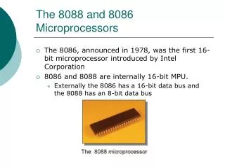
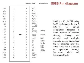
8086 and 8088 Microprocessors • • 8086 announced in 1978; 8086 is a 16 bit microprocessor with a 16 • bit data bus • • 8088 announced in 1979; 8088 is a 16 bit microprocessor with an 8 • bit data bus • • Both manufactured using High-performance Metal Oxide • Semiconductor (HMOS) technology • • Both contain about 29000 transistors • • Both are packaged in 40 pin dual-in-line package (DIP) • • Address lines A0-A7 and Data lines D0-D7 are multiplexed in 8088 • – By multiplexed we mean that the same pysical pin carries an address bit • at one time and the data bit another time • • Address lines A0-A15 and Data lines D0-D15 are multiplexed in • 8086
Minimum-mode and Maximum-mode Systems • • 8088 and 8086 microprocessors can be configured • to work in either of the two modes: the minimum • mode and the maximum mode • Minimum mode: • – Pull MN/MX to logic 1 • – Typically smaller systems and contains a single • microprocessor • Maximum mode • – Pull MN/MX logic 0 • – Larger systems with more than one processor
Minimum-mode and Maximum-mode Systems • Signals common to both minimum and maximum systems
BASIC 8086 MINIMUM MODE SYSTEM MN/MXM/IO INTA RD WR DT/R DEN ALE AD0-AD15 A16-A19 CLK READYRESET 8284A CLOCKGENE-RATOR 8282 LATCH ADDR WAIT STATE GENERATOR 8286 TRAN- CEIVER ADDR/DATA DATA RAM 2142 PERI- PHERAL 2716 PROM
T1 T2 T3 TW T4 CLK M/IO ALE MEMORY ACCESS TIME ADDR/ DATA RESERVED FOR DATA VALID D15-D0 A15-A0 ADDR/ STATUS A19-A16 RD/INTA READY DT/R DEN
T1 T2 T3 TW T4 CLK M/IO ALE ADDR/ DATA A15-A0 DATA OUT (D15-D0) ADDR/ STATUS A19-A16 WR READY DT/R DEN
Minimum Mode Interface • • Address/Data bus: 20 bits vs 8 bits multiplexed • • Status signals: A16-A19 multiplexed with status signals S3-S6 respectively • – S3 and S4 together form a 2 bit binary code that identifies which of the internal segment registers was used to generate the physical address that was output on the address bus during the current bus cycle. • – S5 is the logic level of the internal interrupt enable flag, s6 is always logic 0.
S4 S3 Address status • 0 0 Alternate(relativeto ES segment) • 0 1 Stack (relative to SS Segment) • 1 0 Code/None (relative to CS segment or a default zero) • 1 1 Data (relative to DS segment)
Maximum Mode 8086 System Continued…
Maximum Mode Interface • For multiprocessor environment • • 8288 Bus Controller is used for bus control • • WR¯,IO/M¯,DT/R¯,DEN¯,ALE, INTA¯ signals • are not available • • Instead: • – MRDC¯ (memory read command) • – MWRT¯ (memory write command) • – AMWC¯ (advanced memory write command) • – IORC¯ (I/O read command) • – IOWC¯ (I/O write command) • – AIOWC¯ (Advanced I/O write command) • – INTA¯ (interrupt acknowledge)
Status Bits • They indicate the function of the current bus cycle. They are normally decoded by the 8288 bus controller
– The signals shown above are produced by 8288 depending on the state of S0, S1 and S2. • • DEN, DT/R¯ and ALE signals are the same as minimum-mode systems • • LOCK¯: when =0, prevents other processors from using the bus • • QS0 and QS1 (queue status signals) : informs about the status of the queue • • RQ¯/GT ¯0 and RQ¯/GT ¯1 are used instead of HOLD and HLDA lines in a multiprocessor environment as request/grant lines.
Memory Read timing in Maximum Mode Here MRDC* signal is used instead of RD* as in case of Minimum Mode S0* to S2* are active and are used to generate control signal.
INTERRUPT The meaning of ‘interrupts’ is to break the sequence of operation.While the cpu is executing a program,on ‘interrupt’ breaks the normal sequence of execution of instructions, diverts its execution to some other program called Interrupt Service Routine (ISR).After executing ISR , the control is transferred back again to the main program.
Type 4 POINTER (OVERFLOW) 010H Type 3 POINTER (BREAK POINT) 00CH Type 2 POINTER (NON-MASKABLE) 008H Type 1 POINTER (SINGLE STEP) 004H Type 0 POINTER (DIVIDE ERROR) 000H 16 bits Interrupt Vector Table
03FFH Type 255 (Available) 03FCH Available Interrupts (224) Type 32 (Available) 080H Type 31 (Reserved) 07FH Reserved Interrupts (27) 0014H Type 5 Reserved
Interrupt Vector Table INT Number Physical Address INT 00 00000 INT 01 00004 INT 02 00008 : : : : INT FF 003FC
Example Find the physical address in the interrupt vector table associated with • INT 12H b) INT 8H Solution: a) 12H * 4 = 48H Physical Address: 00048H ( 48 through 4BH are set aside for CS & IP) b) 8 * 4 = 20H Memory Address : 00020H
Functions associated with INT00 to INT04 (Exceptions) INT 00 (divide error) • INT00 is invoked by the microprocessor whenever there is an attempt to divide a number by zero • ISR is responsible for displaying the message “Divide Error” on the screen
Ex1: Mov AL,82H ;AL= 82 SUB CL,CL ;CL=00 DIV CL ;82/0 = undefined result EX2: Mov AX,0FFFH; AX = FFFFH Mov BL,2 ; BL=02 DIV BL ; 65,535/2 = 32767 larger than 255 maximum capacity of AL
INT 01 • For single stepping the trap flag must be 1 • After execution of each instruction, 8086 automatically jumps to 00004H to fetch 4 bytes for CS: IP of the ISR
8086 NMI 5v INT 02 (Non maskable Interrupt) When ever NMI pin of the 8086 is activated by a high signal (5v), the CPU Jumps to physical memory location 00008 to fetch CS:IP of the ISR assocaiated with NMI
INT 03 (break point) • A break point is used to examine the cpu and memory after the execution of a group of Instructions. • It is one byte instruction whereas other instructions of the form “INT nn” are 2 byte instructions.
INT 04 ( Signed number overflow) • There is an instruction associated with this INT 0 (interrupt on overflow). • If INT 0 is placed after a signed number arithmetic as IMUL or ADD the CPU will activate INT 04 if 0F = 1. • In case where 0F = 0 , the INT 0 is not executed but is bypassed and acts as a NOP.
0100 0000 +64 0100 0000 +64 1000 0000 +128 Example Mov AL , 64 Mov BL , 64 ADD AL , BL INT 0 ; 0F = 1 • INT 0 causes the cpu to perform “INT 04” and jumps to physical location 00010H of the vector table to get the CS : IP of the ISR
HARDWARE INTERRUPTS • NMI : Non maskable interrupts • INTR : Interrupt request Edge triggered Input NMI INTR INTA 8086 Level triggered Input Response to INTR input
Hardware Interrupts NMI: TYPE 2 Interrupt INTR: Between 20H and FFH
The Math Coprocessor:8087(Numeric Data Processor (NDP)) • The 8086 performs integer math operations • Floating point operations are needed, e.g. for Sqrt (X), sin (x), etc. • These are complex math operations that require large registers, complex circuits, and large areas on the chip • A general data processor avoids this much burden and delegates such operations to a processor designed specifically for this purpose -e.g. math coprocessor (8087) for the 8086 • The 8086 and the 8087 coprocessors operate inparallel and share the busses and memory resources • The 8086 marks floating point operations as ESC instructions, will ignore them and 8087 will pick them up and execute them
ARCHITECTUTRE • CONTROL UNIT • EXECUTION UNIT

![8086 [2]](https://cdn1.slideserve.com/2457127/8086-2-dt.jpg)