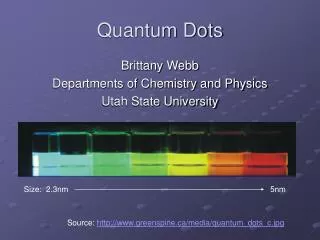
EXPLORING QUANTUM DOTS
EXPLORING QUANTUM DOTS. By Amit Kumar Sharma Sai Krishna Priyanka Gupta. What are QDs. Quantum dots are nano sized semiconductor embedded in another semiconductor. They are capable of trapping discreet number of electron in a point structure. They are approx. of the size of 30nm.

EXPLORING QUANTUM DOTS
E N D
Presentation Transcript
EXPLORING QUANTUM DOTS By Amit Kumar Sharma Sai Krishna Priyanka Gupta
What are QDs • Quantum dots are nano sized semiconductor embedded in another semiconductor. • They are capable of trapping discreet number of electron in a point structure. • They are approx. of the size of 30nm. • They have energy band gaps smaller than that of surrounding materials, hence they trap charge carriers. • The number can be changed by changing the surrounding electric field.
Types of Quantum Dots Quantum dots are basically of two types:- a) Gated quantum dots. b) Self growing quantum dots.
Gated Quantum Dots • These are quantum dots that are at present fabricated using lithography followed by etching. • Success of this method is limited because of technological requirement of producing ultra small structure that are defect free.
Self growing Quantum Dots • In this type a layer of semi conductor over another thin layer of semiconductor material is spread. • Due to difference in lattice, stress is produced which lead to formation of QDs called ‘self growing quantum dots’. • They eliminate the limitation of ‘Gated -QDs’
How Quantum Dots Work
Gated QDs Fabrication • Silicon nano structures are used . • Using of Silicon on insulator (SOI) bring the size down to 5nm. • Using high resolution low energy electron beam Lithography we prepare Silicon dot structure. • Simultaneously the in plane side gate is formed in thin SOI film.
Gated QDs Fabrication • The etched Silicon is passivated at low temperature. • Contact holes opened in source and drain region by etching. In this way gated quantum dots are fabricated
Self grown QDs fabrication • Several layers of silicon germanium are arranged in regular arrays. • Due to lattice mismatch between different layers regularly spaced or sized clusters are formed. • They form Si-Ge quantum dots pyramid shaped clusters, which are 100nm wide and 3-10 nanometer tall. • Once the process is initiated they develop self growing tendency hence the name.
Applications Quantum dots find a number of application in various fields, the most important of them is in field of telecommunication and computing.
Applications Quantum Cells - The Basic Unit • A number of QDs can be used to form a cell which is the basic unit. • Each cell will have 4 QDs . • In each cell there will be two electrons which occupy the dots in such a way that they are in lowest energy states. • These two states can be used as two states of digital signal (0 and 1).
Applications Quantum Cells - The Basic Unit
Applications Quantum Cells - The Basic Unit The two states can be used as two states of digital signal (0 and 1).
Applications Quantum Wires The Quantum-cells can be used to transmit signals just as in a wire.
Applications Direction of signal propogation
Applications Direction of signal propogation
Applications Direction of signal propogation
Applications Direction of signal propogation
Applications Direction of signal propogation
Applications Direction of signal propogation
Applications 1 Direction of signal propogation
Applications Quantum Wires Advantages: • Practically no heat dissipation. • Signal remains unaffected by surrounding EM fields. Hence no signal attenuation takes place • No insulation required. • Massive reduction in size.
Applications Implementing Logic Gates • Logic gates can be implemented using QDs. • QD logic gates -three input gates. • Majority gates