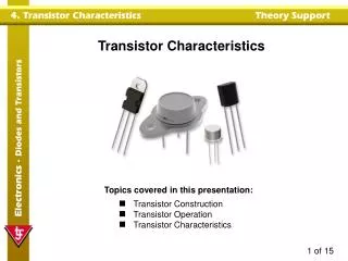
Transistor Characteristics
Transistor Characteristics. Topics covered in this presentation: Transistor Construction Transistor Operation Transistor Characteristics. The Transistor. The transistor is a semiconductor device that revolutionised electronics in the 1950s and 60s.

Transistor Characteristics
E N D
Presentation Transcript
Transistor Characteristics • Topics covered in this presentation: • Transistor Construction • Transistor Operation • Transistor Characteristics
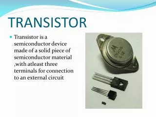
The Transistor The transistor is a semiconductor device that revolutionised electronics in the 1950s and 60s. Although individual transistors have been replaced in many applications, transistors are still used in power gain applications. They can be found in driver circuits where the signal from an input or a process is not powerful enough to drive the output device. There are many different types of transistors, but in this assignment we will examine only the bipolar junction transistor. Today, transistors are used in integrated devices where several thousand transistors are formed in a single device.
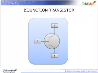
Bipolar Junction Transistor The bipolar junction transistor is a semiconductor device containing two p-n junctions. To form the two junctions, the semiconductor material is arranged in three layers. This allows two different types of transistor to be created, depending on the order of the n-type and p-type semiconductor layers. The two types of bipolar junction transistors are NPN and PNP, although only the NPN transistor will be considered in this module.
Bipolar Junction Transistor The three layers are called the base, emitter, and collector. Base (B) - The base is the middle layer of semiconductor material and controls the flow of charge carriers between the emitter and the collector. Emitter (E) - The emitter region is heavily doped with charge carriers that can be emitted into the base. Collector (C) - The collector is lightly doped so that it can collect charge carriers from the base region.
Bipolar Junction Transistor Each type of bipolar junction transistor has its own circuit symbol showing the base, emitter and collector. The arrow on the symbol always appears on the emitter terminal and points from P to N. For an NPN transistor, the arrow on the emitter will point outwards.
NPN Transistor Biasing The bipolar junction transistor contains two pn junctions that behave exactly like a diode. Each junction must be correctly biased to allow electrons to flow between the emitter and collector. For this reason, an NPN transistor cannot be replaced by a PNP transistor.
NPN Transistor Biasing For an NPN transistor, to allow the electrons in the emitter to move to the base, the voltage at the base must typically be 0.6V higher than the voltage at the emitter. To allow these electrons to continue on to the collector, the collector voltage must be higher than the base voltage. Although some of the electrons will exit the transistor at the base, the majority of them will continue onto the collector.
Transistor Characteristics When selecting a transistor for an application, there are three main characteristics that must be taken into account. These are generally plotted as graphs. • Input Characteristic • Base current (IB) against base-emitter voltage (VBE) • Output Characteristic • Collector current (IC) against collector-emitter voltage (VCE) • Transfer Characteristic • Collector current (IC) against base current (IB)
Input Characteristic The input characteristic is a plot of base current (IB) against base-emitter voltage (VBE) for a fixed collector-emitter voltage. From this graph you can determine what voltage must be applied across the base and emitter in order to switch on the transistor.
Output Characteristic The output characteristic is a plot of collector current (IC) against collector-emitter voltage (VCE) for a range of base currents. The graph shows a series of plots, one for each base current value. From the graph it can be seen that initially the collector current varies greatly for small change to the collector emitter voltage. At this point the transistor is not very stable.
Output Characteristic However, above a certain value the collector-emitter voltage has little effect on the collector current (for a given base current) and the transistor becomes more stable. The transistor is generally operated in this stable region, and the output characteristic graph shows what minimum value of collector-emitter voltage must be applied to keep it operating in the stable region.
Transfer Characteristic The transfer characteristic shows the collector current against base current at a fixed value of collector-emitter voltage. For a given collector-emitter voltage the graph will be approximately linear, which shows that the base current is almost a constant fraction of the collector current. The transistor acts as a current amplifier. The ratio of collector current to base current is called the DC current gain (hFE). The value of DC current gain varies between transistors - even between transistors of the same type.
Transistor Datasheet Some of the criteria, found on the product data sheet, to consider when selecting a transistor. • DC current gain • Collector-emitter breakdown voltage • Collector-emitter saturation voltage • Base-emitter ‘on’ voltage • Package Type
Transistor as a Switch If the base-emitter voltage is below 0.6V, the transistor will not conduct, resulting in no base current and no collector current. A base current is required to obtain a collector current. By switching the base current on and off, the collector current can also be switched on and off. The transistor can therefore be used as a switch with the base current controlling the flow of the collector current.
Practical Transistor Switch Circuit In a practical transistor switch circuit the load is connected between the collector and the positive supply rail. A resistor is connected between the base and the power supply. This is to ensure that the current through the base-emitter junction is kept to a safe level, in order to prevent damage to the transistor.