Download
1 / 58
580 likes | 695 Vues
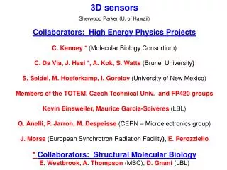
3D sensors Sherwood Parker (U. of Hawaii) Collaborators: High Energy Physics Projects C. Kenney * (Molecular Biology Consortium) C. Da Via, J. Hasi *, A. Kok, S. Watts (Brunel University ) S. Seidel, M. Hoeferkamp, I. Gorelov (University of New Mexico)

E N D
3D sensors Sherwood Parker (U. of Hawaii) Collaborators: High Energy Physics Projects C. Kenney *(Molecular Biology Consortium) C. Da Via, J. Hasi *, A. Kok, S. Watts(Brunel University) S. Seidel, M. Hoeferkamp, I. Gorelov(University of New Mexico) Members of the TOTEM, Czech Technical Univ. and FP420 groups Kevin Einsweiler, Maurice Garcia-Sciveres (LBL) G. Anelli, P. Jarron, M. Despeisse (CERN – Microelectronics group) J. Morse(European Synchrotron Radiation Facility), E. Perozziello * Collaborators: Structural Molecular Biology E. Westbrook, A. Thompson (MBC), D. Gnani (LBL)
Outline: Pixels – replacement / upgrade • 1. what is needed • 2. basic 3D properties • 3. how they help • 4. results – first irradiation • 5. results – speed, active edges • 6. results – ATLAS front end chip • 7. results – second irradiation • 8. improved yield: planar/3D active edges • 9. improving yield: current run • 10. ongoing measurements
From: B-Layer Replacement Proposal, Goals K. Einsweiler, LBNL December Pixel Week, 2004 Scope: •Therefore propose that new B-layer have design goal of 3 times design luminosity both for total dose lifetime and for instantaneous luminosity tolerance. For total dose, assume that a similar several year lifetime is needed, so this would translate to about 3 x 10¹⁵ n equivalent NIEL dose and 150 MRad ionizing dose. •Of course if this proves too difficult, we can always build several B-Layers using the present technology, and change them each year or two.
Material Reduction: •Basic cooling services would remain unchanged, so reductions must come from electrical services, and from minimizing overlap fractions by maximizing the active fraction of the pixel module. •Present module has active fraction of 71%. With larger FE die size, a design optimized to minimize non-active region at bottom of FE chip, and an edgeless sensor technology, could increase the active fraction to about 90%. ATLAS Pixel B-Layer Replacement Proposal ATL-IP-ER-0015 Modified: 30/12/2004 Rev. No.: 2.0 3.3 Sensor technology: . . . .We expect that, including the effects of charge sharing between pixels, a minimum signal size of 8-10Ke will be required in order to achieve greater than 99% single-hit efficiency for the B-Layer.
Outline: Pixels – replacement / upgrade • 1. what is needed • 2. basic 3D properties • 3. how they help • 4. results – first irradiation • 5. results – speed, active edges • 6. results – ATLAS front end chip • 7. results – second irradiation • 8. improved yield: planar/3D active edges • 9. improving yield: current run • 10. ongoing measurements
INTRODUCTION NIMA 395 (1997) 328 IEEE Trans Nucl Sci 46 (1999) 1224 IEEE Trans Nucl Sci 48 (2001) 189 IEEE Trans Nucl Sci 48 (2001) 1629 IEEE Trans Nucl Sci 48 (2001) 2405 CERN Courier, Vol 43, Jan 2003, pp 23-26 NIMA 509 (2003)86-91 NIMA 524 (2004) 236-244 3D silicon detectors were proposed in 1995 by S. Parker, and active edges in 1997 by C. Kenney. Combine traditional VLSI processing and MEMS (Micro Electro Mechanical Systems) technology. Electrodes are processed inside the detector bulk instead of being implanted on the Wafer's surface. The edge is an electrode! Dead volume at the Edge < 2 microns! Essential for -Large area coverage -Forward physics
(signal strength from infra red light beam) n n n n p p + 100 µm 134 µm n n n n 200 µm 100 µm n-type bulk
Speed: planar 3D 4. 4. 4. 1. 3D lateral cell size can be smaller than wafer thickness, so 2. in 3D, field lines end on cylinders rather than on circles, so 3. most of the signal is induced when the charge is close to the electrode, where the electrode solid angle is large, so planar signals are spread out in time as the charge arrives, and 4. Landau fluctuations along track arrive sequentially and may cause secondary peaks (see next slide) 5. if readout has inputs from both n+ and p+ electrodes, 6. for long, narrow pixels and fast electronics, • shorter collection distance • higher average fields for any given maximum field (price: larger electrode capacitance) • 3D signals are concentrated in time as the track arrives • Landau fluctuations arrive nearly simultaneously • drift time corrections can be made • track locations within the pixel can be found
Potential 3D features from preliminary calculations: p 50 µm 8 µm n 50 µm 1 ns 3 ns 3. Fast pulses. Current to the p electrode and the other 3 n electrodes. (The track is parallel to the electrodes through a cell center and a null point. V – bias = 10V. Cell centers are in center of any quadrant. Null points are located between pairs of n electrodes.)
Outline: Pixels – replacement / upgrade • 1. what is needed • 2. basic 3D properties • 3. how they help • 4. results – first irradiation • 5. results – speed, active edges • 6. results – ATLAS front end chip • 7. results – second irradiation • 8. improved yield: planar/3D active edges • 9. improving yield: current run • 10. ongoing measurements
Useful properties of 3D radiation sensors: • 1 Long tracks can have short drift distances. • 2 They can be depleted, and have full sensitivity, at lower bias voltages. • 3 The geometric nature of this means there will be a low increase of depletion voltage with radiation damage. • 4 They have rapid charge collection, and charges from perpendicular tracks come in together, rather than one at a time from the track ends, so they can make order-of-magnitude shorter pulses.
5. This speed is maintained, as expected, in heavily irradiated sensors, and is useful in reducing capture losses regardless of amplifier speeds. 6. With fields directed away from, rather than along pixel or strip boundaries, they have reduced charge-sharing. Charge-sharing may be used to improve spatial resolution, but may also take tracks below threshold in radiation damaged silicon, particularly with planar sensors.
7. Active edges provide full sensitivity to within a few microns of the physical edges, in contrast with the large dead regions of standard planar technology (1.1 mm in the Atlas and CMS pixel sensors which must allow for many concentric guard rings). 8. Bias voltages can be made to vary across 3D sensors. (useful if radiation damage and so depletion voltages are much higher at, for example, sensor edges near the beam)
BUT they require more fabrication work.
Outline: Pixels – replacement / upgrade • 1. what is needed • 2. basic 3D properties • 3. how they help • 4. results – first irradiation • 5. results – speed, active edges • 6. results – ATLAS front end chip • 7. results – second irradiation • 8. improved yield: planar/3D active edges • 9. improving yield: current run • 10. ongoing measurements
Probe point R - probe C - probe C - sensor V - bias
3D performance after irradiation 90-Sr βsignal in 3D sensor irradiated by 10e15 SPS protons / sq cm, fully reverse annealed, no implanted oxygen, room temperature. IR µbeam signal vs. V-bias, 3D sensor 10e15 55 MeV protons / sq. cm ≈ 1.8 10e15 1 MeV neutrons. Measured at room temp. Stored at low temp. No beneficial or reverse annealing, no oxygen. Both sensors 181 µm thick, 100 µm × 134 µm cells, joined in rows for readout.
Outline: Pixels – replacement / upgrade • 1. what is needed • 2. basic 3D properties • 3. how they help • 4. results – first irradiation • 5. results – speed, active edges • 6. results – ATLAS front end chip • 7. results – second irradiation • 8. improved yield: planar/3D active edges • 9. improving yield: current run • 10. ongoing measurements
0.13 µm chips now fabricated – rise, fall times expected to be ≈ 1.5 ns rise times ≈ 3.5 ns fall times ≈ 3.5 ns Resistive (transistor channel) feedback, and so a current amplifier.
90Sr.20v.bias3.1 4.00E-03 30ns 2.00E-03 0.00E+00 1 23 45 67 89 111 133 155 177 199 221 243 265 287 309 331 353 375 397 419 441 463 485 507 529 551 573 595 617 639 661 683 705 727 749 771 793 -2.00E-03 5ns v -4.00E-03 -6.00E-03 -8.00E-03 -1.00E-02 time (62.5 ps / point) 0.13 µm transimpedance amplifier, 90-Sr β source, no collimation channel 1 self-triggers, other two channels are left, right neighbors Time Pts: channel 1 channel 2 channel 3
30ns 5ns 0.13 µm transimpedance amplifier, 90-Sr β source, no collimation channel 1 self-triggers, other two channels are left, right neighbors
30ns 5ns 0.13 µm transimpedance amplifier, 90-Sr β source, no collimation channel 1 self-triggers, other two channels are left, right neighbors
30ns 5ns
5ns Amplifier output, 0.8 ns rise-time step pulse applied to input.
space for guard rings • sawed edges connecting top and bottom are conductors • chips and cracks are also conducting and can reach inside the edges • the field lines bulge out, and should be kept away from b and cs a b d c Reasons for dead borders on standard planar technology sensors
etch border trenches • diffuse in dopant • grow protective oxide cover • fill trench with poly • vertical, directed etch (to dotted lines) • turn off sidewall protection step • isotropic etch to oxide stop • additional steps are not included on this slide (and note, bonding oxide to support wafer not colored ) • n and p electrodes can be reversed oxide p p n n sensor wafer oxide support wafer p p n n support wafer oxide Active Edges
d D Some work on deep etching: 0. An old hole (filled). D/d = 121 µm /11µm. • Process steps to improve depth / diameter ratios, and to make holes and trenches at the same time (middle). Note: s(↕) = s(↔) × cos 20º. • True diameter from an angled saw cut: (right). D/d, top holes ≈ 18 / 1. • A second, newer STS etcher has just been installed at Stanford. It is faster and should make somewhat narrower holes and trenches. • The old etcher will become a “dirty” one, allowing us to make trench “dicing” etches on wafers with indium bumps.
inter-strip boundaries edge X-ray microbeam results for a 3D sensor X-ray micro-beam scan, in 2 µm steps, of a 3D, n bulk and edges, 181µm thick sensor. The left curve is for the edge p channel. The horizontal scale is in µm; the vertical is arbitrary. The small dip in each center is from nearby 3D electrodes. The left edge tail is from reflected gold x-rays and from leakage current.
Current from scan in an x-ray microbeam, of another 3D sensor with a photomicrograph of the corresponding part on the right. Grid lines are spaced 10µm apart.
Some results from the CERN X5 beam test (120 GeV muons) Measured hit position in 3D sensor plane #3 vs. predicted position from beam telescope. Fitted 3D sensor width = 3,203 ±4 µm. Drawn width = 3,195 µm. Sensor efficiency = 98%. System efficiency less due to DAQ, triggering electronics.
Outline: Pixels – replacement / upgrade • 1. what is needed • 2. basic 3D properties • 3. how they help • 4. results – first irradiation • 5. results – speed, active edges • 6. results – ATLAS front end chip • 7. results – second irradiation • 8. improved yield: planar/3D active edges • 9. improving yield: current run • 10. ongoing measurements
More typical spectrum TOT spectrum for the best looking pixel • Possible steps for improvement of fabrication yields: • Improvement of fabrication steps (as was done for planar / 3D active edge sensors). • Use solder bumps at wafer scale. • 2-3 month fabrication run rather than 5 week run. • Use of P- type bulk so diode junctions always at signal electrodes so one bad junction does not short bias supply. • Probably won’t need to reduce signal electrode capacitance using poly-resistor isolation of bias electrodes, but it remains a possibility.
Outline: Pixels – replacement / upgrade • 1. what is needed • 2. basic 3D properties • 3. how they help • 4. results – first irradiation • 5. results – speed, active edges • 6. results – ATLAS front end chip • 7. results – second irradiation • 8. improved yield: planar/3D active edges • 9. improving yield: current run • 10. ongoing measurements
total n p other charged hadrons
Second Irradiation Irradiation and thermal history of the samples. The samples were irradiated with 10MeV reactor neutrons. The integration and scaling of the spectrum gave a 1MeV equivalent damage factor of 1.8. The required, resulting, measured by the dosimeter, and the corrected fluences are respectively: requested resulting corrected [n/cm^2] [n/cm^2] [n1MeV eq/cm2] 1e16 4.78e15 8.6 e15 7D 5e15 3.32e15 5.98 e15 7A 3e15 2.08e15 3.74 e15 7F 1e15 8.19e14 1.47e15 7E (unstable before irradiation) 5e14 3.57e14 6.43 e14 1B Vladimir Linhart, Tomas Slavicek and Tomas Horadzov: Praha. C. Da Via’, Brunel. Sample fabricated and checked by J. Hasi and C. Kenney at Stanford Irradiation organised by S. Pospisil, Praha, . Useful discussions with S. Parker, Hawaii and S. Watts, Brunel.
0.64 3.7 6.0 8.6 xe15 Preliminary calculation of the α parameter for a volume of 0.418 mm2 is 3.8 x10⁻¹⁷. This assumes the leakage current to be generated by the device full physical volume.
Oscilloscope trace of an alpha particle with the corresponding histogram (generated automatically by the oscilloscope), measured at –15C using the sample 7F with 140V bias. The vertical scale is 500mV/div.
90Sr source, self triggered. 7F at –15C. at 140V bias (3.74e15 n/cm^2). Oscilloscope traces of 3 beta particles measured under the same conditions and with the same detector. The vertical scale is 50mV/div.
Outline: Pixels – replacement / upgrade • 1. what is needed • 2. basic 3D properties • 3. how they help • 4. results – first irradiation • 5. results – speed, active edges • 6. results – ATLAS front end chip • 7. results – second irradiation • 8. improved yield: planar/3D active edges • 9. improving yield: current run • 10. ongoing measurements