
Introduction to Data Conversion
E N D
Presentation Transcript
Introduction to Data Conversion EE174 – SJSU Tan Nguyen
Introduction to Data Conversion • Introduction to ADC and DAC • DAC specifications • ADC specifications • Types of ADCs and DACs • Limitations of ADC and DAC in high frequency applications • Trade off
Vocabulary • ADC (Analog-to-Digital Converter): converts an analog signal (voltage/current) to a digital value. • DAC (Digital-to-Analog Converter): converts a digital value to an analog value (voltage/current). • ADC sampling time: A sampling capacitor must be charged for a duration of Tsample before conversion taking place. • Full Scale output (VFS) and Reference voltage (Vref): Analog signal varies between 0 and Vref, or between +/-Vref. Note: VFS = Vref– 1LSB. • Resolution: Number of bits (N-bits) used for conversion. The higher bits, the more precise is the digital output. • Conversion Time: Time taken to convert the voltage on the sampling capacitor to a digital output. • Quantization is the process of converting a continuous range of values into a finite range of discreet values. This is a function of ADC, which create a series of digital values to represent the original analog signal. • The quantization error of an ideal ADC is half of the step size (1 LSB). • Differential Nonlinearity (DNL) error is the difference between an actual step width (for an ADC) or step height (for a DAC) and the ideal value of 1 LSB. • Integral Nonlinearity (INL) error is the deviation of the values on the actual transfer function from a straight line. • Effective Number Of Bits (ENOB) is a measure of the dynamic performance of an ADC.
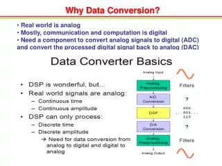
Why Data Conversion? • In processing and communication there are only two types of data forms: analog and digital data. • Data Conversion is the process of changing or converting one form of data in to another form. • Real world signals (temp, pressure, position, sound, light, speed, etc.) are analog signals: • Continuous time and continuous amplitude • Noisy and difficult to store • Digital processors can only process digital signals which are: • Discrete time and discrete amplitude • Binary data can be easily to store • In order to interface digital processors with the analog world, data acquisition and reconstruction circuits must be used: analog-to-digital converters (ADCs) to acquire and digitize the analog signal at the front end, and digital-to-analog converters (DACs) to reproduce the analog signal at the back end. • Digital data conversion system requires ADC and DAC. • Typical Data Conversion System
Analog-to-Digital Converter (ADC) The analog-to-digital converter (ADC) converts a continuous-amplitude, continuous-time input to a discrete-amplitude, discrete-time signal. An analog low-pass (anti-alias) filter removes any high frequency components that may cause an effect known as aliasing. The filter output signal is sampled at a rate of fS samples per second to produce a discrete-time signal. The amplitude of this discrete-time signal is "quantized," i.e., approximated with a level from a set of fixed references, thus generating a discrete-amplitude signal. The discrete-amplitude signal is decoded to a digital representation of that level is established at the output. Note: ADCs usually require the input be held constant during the conversion process, indicating that the ADC must be preceded by an Sample-and-Hold Amplifier (SHA) to freeze the band-limited signal just prior to each conversion.
Digital-to-Analog Converter (DAC) The digital data is processed by a digital processor and output to the digital-to analog converter (DAC). The DAC reverses the ADC process, it converts a discrete time, discrete amplitude into continuous time, continuous amplitude. The DAC is usually operated at same frequency as the ADC. A DAC selects and produces an analog level from a set of fixed references according to the digital input. If the DAC generates large glitches during switching from one code to another, a "deglitching" circuit (usually a sample-and-hold amplifier) follows to mask the glitches. The reconstruction function performed by the DAC introduces sharp edges in the waveform as well as a sine envelope in the frequency domain, an inverse-sine filter and a low-pass filter are required to suppress these effects. The resulting staircase-like signal is finally passed through a smoothing filter to ease the effects of quantization noise. Note: The de-glitchermay be removed if the DAC is designed to have small glitches. Also, the inverse sine filtering may be performed before DAC conversion in the digital domain.
ADC Process: Sampling Theorem • The fundamental consideration in sampling is how fast to sample a signal to be able to reconstruct it. • Suppose a signal’s highest frequency is fmax. Then a proper sampling requires a sampling frequency fsat least satisfying • As sampling rate increases, sampled waveform looks more and more like the original. • Sampling rate less than Nyquist rate results in original signal is not recovered known as aliasing phenomenon. fs> 2fmaxNyquist rate = 2 fmax Nyquist frequency = fs/2 Aliasing Example 1: Given the signal v(t) = 7 + 5cos(2π440t) + 3sin(2π880t) , what is the proper sampling rate? Solution: The proper sampling rate fs > fNyquist= 2(880)=1760 Hz. Analog sinusoid x(t) = A cos(2pf0t+ f) Sample at Ts = 1/fs x[n] = x(Ts n) = A cos(2p f0 Tsn + f) = A cos(ωn n + f) ωn Ͼ [0, p) is called principal alias Keeping the sampling period same, sample y(t) = A cos(2p(f0 + lfs)t + f) where l is an integer y[n] = y(Ts n) = A cos(2p(f0 + lfs)Tsn + f) = A cos(2pf0Tsn + 2p lfsTsn + f) = A cos(2pf0Tsn + 2p l n+ f) = A cos(2pf0Tsn + f) = x[n] y[n] indistinguishable from x[n] or x[n] and y[n] are aliases of each other
ADC Process: Sampling Theorem For a sinusoid signal v(t) = 2sin(200πt) = 2sin(2π100t) is sampled at fs = 1000 Hz > 2 fmax a proper sampling to recover signal. Equivalently, there are 1000/100 = 10 samples per sinewave cycle. Now, if sampling fs = 120 Hz or equivalently there are 1.2 samples per sinewave cycle an improper sampling of the signal because another sine wave can produce the same samples. The original sine misrepresents itself as another sinewave. This phenomenon is called aliasing. • For v(t) = 2sin(200πt) = 2sin(2π100t). • Analysis: • For fs1 = 1000 Hz v1[n] = 2sin(2πn 100/1000) = 2sin(2πn(0.10)) = 2sin(0.2πn) • Recovering signal: vr1(t) = 2sin(0.2π tx1000) = 2sin(200πt) = 2sin(2π 100t) • Signal recovered • For fs2 = 120 Hz vr2[n] = 2sin(2πn 100/120) = 2sin(1.67πn) • = 2sin( (2 – 0.33)πn) = 2sin(– 0.33πn) = – 2sin(0.33πn) • Recovering signal: vr2(t) = – 2sin(0.33πtx120) = – 2sin(39.6πt) • = – 2sin(2π19.8t) Original signal is not recovered Sampling at 10x higher than the highest frequency present in the signal Recovering signal Sampling at 1.2x higher than the highest frequency present in the signal
Illustration of ADC Process • There are two related steps in A-to-D conversion: • Sampling and Holding (S/H): • Converts an analog signal into a discrete-time signal, a sequence of real numbers • S/H circuit is used to sample analog signal at discrete points in time in track mode and hold the discrete value during the hold mode. • Analog voltage sampled at discrete time t is rounded off to nearest discrete voltage value. • Quantization and Encoding: • Quantization replaces each real number with an approximation from a finite set of discrete values. These discrete values are represented as fixed-point words (2-bit, 3-bit, 8-bit, … quantization level). • Each discrete value level is endecoded to a digital code, and the signal is represented as a sequence of digital codes which can be stored the in memory for future processing. S H S H S H S H S H S
ADC Process: Quantization and Coding • The analog input is an infinite valued quantity and the output is a discrete value, an error will be produced as a result of the quantization. This error, known as quantization error, Qe, is defined as the difference between the actual analog input VIN and the value of the output (staircase) Vstaircasegiven in voltage. It is calculated as: • Qe = VIN – Vstaircase • The greater number of bits, the better precision of the ADC • Round-off error (a.k.a. Quantization error) cannot be recovered and the amount of round-off error decreases with increasing number of bits used in the ADC. • The quantization error of an ideal ADC is half of the step size. • Encoding: Assigning a unique digital code to each quantum, then allocating the digital code to the input signal.
Improve the accuracy in ADC • Increase the resolution which improves the accuracy in measuring the amplitude of the analog signal. • Increase the sampling rate which increases the maximum frequency that can be measured. • Increasing both sampling time and resolution, the difference between the analog and the digital signals would become negligible. 3-bit ADC Higher Resolution Higher Sampling Rate 2-bit ADC
Ideal 3-bit ADC transfer function and staircase with - 1/2 LSB offset • When an ADC converts a continuous signal into a discrete digital representation, there is a range of input values that produces the same output. That range is called quantum (Q) and is equivalent to the Least Significant Bit (LSB). The difference between input and output is called the quantization error. • For an ideal ADC, quantization error is bounded by –Q/2 and +Q/2 for inputs within full-scale range.
ADC Characteristics • An ideal ADC: • Accepts analog input in the form of either voltage or current • Produces digital output either in serial or parallel form • N = # of bits • VFS = Full scale output = Vref – 1 LSB = Vref • = min. resolvable input 1 LSB = • Resolution: • Resolution is the smallest input voltage change a digitizer can capture • Resolution of a N-bit ADC is defined as • Q = where Vref = (Vref+ - Vref-). • If Vref- = 0 V, Vref= Vref+ • ADC Equations: • Given Vin = input voltage and N = number of bits of precision. • Output_code (D) = x 2Nor Vin = x Vref MSB DN-1 DN-2 Output_code D1 D0 LSB Number of quantization levels = 2N Example:
Signal-Noise Ratio (SNR) relates to N-bits in digital presentation • Any value of the error is equally likely, so it has a uniform distribution ranging from −Q/2 to +Q/2. Then, this error can be considered a quantization noise with RMS vqn: Assuming an input sinusoidal with peak-to-peak amplitude Vref, where Vref is the reference voltage of an N-bit ADC (therefore, occupying the full-scale of the ADC), its RMS value is Vrms: To calculate the Signal-Noise Ratio, we divide the RMS of the input signal by the RMS of the quantization noise: SNR = 6.02 xN + 1.76 (dB) This SNR equation generalizes to any system using a digital representation. Accurate for N > 3.
Examples Given Vref = 10V, N=12, and Vin = 9V. Find: (a) the resolution Q (1 LSB), (b) the output_code, (c) the quantization noise vqn, (d) the SNR. Solutions: A 12 bit ADC has a resolution of 212 = 4,096. Therefore, our best resolution is 1 part out of 4,096, or 0.0244% of the Vref or 10V / 212 = 2.44 mV Output_ code = x 2N = x 4096 = 368610 = 0xE66 vqn= = 0.704 mV SNR = 6.02 x N + 1.76 = 6.02 x 12 + 1.76 = 74 dB 2) Given an input voltage Vin = 9V with Vref = 10V. Determine minimum bits (N) would be required to have less than ± 0.5% quantization error? Known: Absolute quantization error |QE| (in mV ) = ± . And, Q = . Solution: = 0.5% = 0.005 |QE| = 9000 mV x 0.005 = 45 mV = Q = 90 mV/bit (LSB) Q = 90 mV/bit = 2N = = ≈ 111 N = ≈ 6.8 so minimum N = 8 because 7-bit DAC not available. Note: Higher N will also work but added cost.
Examples 3) Given Vref = 10V, and a 10-bit A/D output code is 0x12A. a) What is the ADC input voltage? b) If the input voltage is Vin = 2.915 V, what is the output code? c) What is the input voltage range that yield an output code of 0x005? Solution: 1 LSB = Q = 10V / 210 = 0.00976 V = 9.76 mV Q/2 = 4.88 mV a) Vin = output_code / 2N * Vref = (0x12A) / 210 x 5 V = 298/1024 x 10 V = 2.91015 V = 2910.15 mV (ADC Vin) b) For the output code 0x12A, the input voltage range is 2910.15 ± Q/2 or 2905.27 mV < V0x12A < 2915.03 mV So for Vin = 2.915 V the out put code is also 0x12A c) The ideal input voltage to produce output code 5 is V0x005 = 5 x 9.76 mV = 48.8 mV The range for output code 0x005 is 48.8 ± 4.88 mV or 43.92 mV < V0x005 < 53.68 mV
DAC Characteristics • An ideal DAC: • Accepts digital input b1- bN • Produces either analog output voltage or current • N = # of bits • Q = min. step size 1 LSB = • LSB and MSB: • LSB and MSB of a N-bit DAC is defined as • LSB = where Vref = (Vref+ - Vref-) • MSB = If Vref- = 0 V, Vref= Vref+ • N = log2 Resolution • DAC Equations: • Given Vout = output voltage, Vref, N = number of bits of precision • Input_code = x 2Nor Vout = x Vref • Vout_max= Vref – Q = Vref – 1 LSB = Vref ( 1 – )
Ideal Transfer Function DAC DAC: Ideal Transfer Function • Ideal DAC introduces no error! • One-to-one mapping from input to output
Example DAC Computations 3) A design requires step size or LSB = 0.002 V and the reference voltage Vref= 1.6V. a) Determine the minimum resolution N. b) Find the MSB value. c) Find the maximum output Vout_max d) Find the input code for the output voltage Vout = 0.799V Solution: a) N = log2 = log2 = log2(800) = 9.64 N = 10 is minimum requirement b) MSB = = = 0.8V c) Vout_max = Vref – Q = 1.6 – 0.002 = 1.598V d) Input_code = x 2N= x 1024 = 511.36 Input code = 51210 or 0x800
Selecting ADC/DAC • In converting between analog and digital domains errors are introduced. The conversion system must be carefully designed to suit the nature of the signals to prevent these errors affecting the validity of the data. For the more difficult case, of converting from analog to digital data. We need to decide: • The range of the allowed input signal: signal has a range of (v1 - v2) volts. To be certain that the signal will never exceed our ability to convert it we choose a converter with a greater range, say (v3 -v4) volts. • The resolution is the smallest change that we need to measure. • The sampling frequency: How often the signal must be measured to suit the fastest changing part of the signal. • The choice of a DAC is usually limited to the number of bits • required, as all DACs are quite fast. • Having identified the range we require and the resolution to • which we must measure tells us the number of bits required.
Data Converter Performance Metric EE174 – SJSU Tan Nguyen
Data Converter Performance Metrics • Data Converters are typically characterized by static, time-domain, & frequency domain performance metrics : • Static • Offset • Gain error • Full-scale error • Differential nonlinearity (DNL) • Integral nonlinearity (INL) • Monotonicity • Dynamic • Delay & settling time • Aperture uncertainty • Distortion-harmonic content • Signal-to-noise ratio (SNR), Signal-to-(noise+distortion) ratio (SNDR) • Idle channel noise • Dynamic range & spurious-free dynamic range (SFDR)
Static Errors on Converters • Static errors affect the accuracy of the converter when it is converting static (dc) signals. • Each can be expressed in LSB units or a percentage of the FSR. For example, an error of ½ LSB for an 8-bit converter corresponds to approximately 0.2% FSR (½ = 0.1953%). • Offset error • Gain error • Differential nonlinearity (DNL) • Integral nonlinearity (INL) Ideal 3-bit DAC and ADC Transfer Function
ADC Offset and Gain Error • If the transfer function of the actual ADC occurs above the ideal straight line, then it produces positive gain error and vice versa. The gain error is calculated as the number of LSBs from a vertical straight line drawn between the midpoint of the last step of the actual transfer curve and the ideal straight line. • ADC gain error can be calibrated out with hardware or in software. • If the first transition of the actual ADC occurs above the ideal input value of 0.5 LSB, then it produces an positive offset error and vice versa. ADC offset error is calculated as the number of LSBs from the ideal input value of 0.5 LSB. • ADC offset error can be removed be measuring a reference point and subtracting that value from future samples.
Offset Error Example Offset Error value is usually specified using one of the following units: Volts, Least Significant Bits (LSB), %Full Scale Value (%FSV), and parts per million (ppm). For the above example, you can convert between different units as shown in the following example. Calculate a 3 LSB offset error conversion to Volts: Offset Error (V) = Error in LSB × Maximum Input / (2N) Offset Error (V) = 3 × 5 V / (216) FSV = 5V, N=16 Offset Error (V) = 0.000229, that is, 229 μV spacer Offset Error (%FSV) = Offset Error (V) × 100 / Full scale value Offset Error (%FSV) = 0.00458% in term of ppm, with regard to full scale voltage, is Offset Error (ppm FSV) = 46 ppm Though the offset error is usually specified at 25°C in the data sheets, the offset does vary with temperature. The variation in offset is specified as Offset Drift and denoted as ppm/°C. The actual offset at any temperature can be calculated by adding the drift to offset value calculated for room temperature. For the above example if the drift is specified as 1 ppm/°C of REF V. Offset at 85°C = 229 μV + [(85 – 25) × 5 μV] = 529 μV.
Gain Error Example • For an ADC, if the gain error is 4 LSB, then it can be converted to Volts as follows: • • Gain Error (Volts) = Error in LSB × Maximum Input / (2N) • • Gain Error (Volts) = 4 × 5 / (216) = 0.000305 V, that is, 305 μV • This means the ADC will reach 0xFFFF code for input voltage of 4.999656 V. • If the gain error is –4 LSB, then the device will reach 0xFFFF code for input voltage 5.000267 V. • • Gain Error (%FSV) = Gain Error (V) × 100 / Full scale value • • Gain Error (%FSV) = 0.0061% • Similar to offset error, the gain error is usually specified at 25°C in the data sheets and the gain also varies with temperature. The variation in gain is specified as Gain Drift and denoted as ppm/°C. The actual gain error at any temperature can be calculated by adding the drift to gain error value calculated for room temperature. • For the above example, if the drift is specified as 1 ppm/°C of REF V. • Gain Error at 85°C = 305 μV + [(85 – 25) × 5 μV] = 605 μV.
ADC Differential Non-Linearity (DNL) DNL - Differential Non-Linearity: is defined as the difference between the the actual code width of a nonideal ADC and the ideal case. It is expressed as LSB counts. DNL is a function of each ADC's particular architecture. It is not possible to remove its effects with calibration. DNL = Actual step width – Ideal step width Example: Calculate the differential nonlinearity in term of LSB, voltages, % FSR of the 3-bit ADC. Assume that VREF = 8V. Solution: 1 LSB = 8V / 23 = 1 V FSR = VREF – 1 LSB = 8V – 1V = 7V 0.5 V / 7 V = 0.0714 = 7.14% DNL1 = 1.5 LSB – 1 LSB = 0.5 LSB = 0.5V = 7.14% FSR DNL2 = 0.5 LSB – 1 LSB = –0.5 LSB = –0.5 V = –7.14% FSR DNL3 = 1 LSB – 1 LSB = 0 DNL4 = 0 LSB – 1 LSB = –1 LSB = –1 V = –14.28% FSR DNL5 = 2 LSB – 1 LSB = 1 LSB = 1 V = 14.28% FSR DNL6 = 1 LSB – 1 LSB = 0
ADC DNLError • Fig. 2: 0x800 code width is 0 LSB (Missing code). • DNL = – 1 LSB. • Since 0x800 is missing, the ADC cannot be used for high precision applications. Fig. 1: Wide code width Fig. 2: Missing code Fig. 1: The 0x800 code width is 2 LSB (Wide code width). DNL = +1 LSB. • In Fig. 4: The 0x800 code width is – 0.25 LSB (undefined/non- monotonic). • DNL = – 1.25 LSB. • It is clear that the ADC is highly nonlinear. • Fig. 3: The 0x800 code width is 0.25 LSB (Narrow code width). • DNL = – 0.75 LSB , • Since the 0x800 is still there, the ADC can be used in precision applications. Fig. 4: Non-monotonic Fig. 3: Narrow code width
ADC Integral Non-Linearity (INL) INL - Integral Non-Linearity: DNL errors accumulate to produce a total Integral Non-Linearity (INL). It is defined as the maximum deviation from the ideal slope of the ADC and is measured from the center of the step. It is expressed as counts. INL is a function of each ADC's particular architecture. It is not possible to remove its effects with calibration. Notice: For end-point corrected measurement INL[0] undefined INL[1]=0 INL[2N-1]=0 k–1 INL (k) = ∑ DNL[i] i = 1
DAC Offset and Gain Error • The gain error of a DAC indicates how well the slope of an actual transfer function matches the slope of the ideal transfer function after the offset error has been calibrated out. • Gain error is usually expressed in LSB or as a percent of full-scale range (%FSR), and it can be calibrated out with hardware or in software. • For a DAC, offset error is the analog output voltage response to an input code of all zeros.
DNL and INL of DAC • In a DAC, we are concerned with two measures of the linearity of its transfer function: integral nonlinearity, INL (or relative accuracy), and differential nonlinearity, DNL. • Differential nonlinearity (DNL) error is the difference between the ideal and the measured output responses for successive DAC codes. An ideal DAC response would have analog output values exactly 1LSB apart (DNL = 0). • DNL specs ≥ 1LSB guarantees monotonicity in DAC • If the differential nonlinearity is more negative than –1 LSB, the DACs transfer function is non-monotonic. • DNLn = Actual increment height of transition n – Ideal increment height • Integral nonlinearity (INL) is the maximum deviation, at any point in the transfer function, of the output voltage level from its ideal value—which is a straight line drawn through the actual zero and full-scale of the DAC. • INL at the 101 code: DNL001 + DNL010 + DLN011 + DNL100 + DNL101 = 0 + 1.5 + 0 – 3 + 0 = –1.5 LSBs.
ADC Differential Non-Linearity (DNL) • Example: • Calculate the differential nonlinearity in term of LSB, voltages, % FSR of the 3-bit DAC. Assume that VREF = 8V. • Solution: • 1 LSB = 8V / 23 = 1 V • FSR = VREF – 1 LSB = 8V – 1V = 7V • 0.5 V / 7 V = 0.0714 = 7.14% • DNLn= Actual increment height of transition n-Ideal increment height • DNL1, DNL2and DNL7= 1 LSB -1 LSB = 0 • DNL3=1.5 LSB -1 LSB = 0.5 LSB • DNL4= 0.5 LSB -1 LSB = -0.5 LSB • DNL5= 0.25 LSB -1 LSB = -0.75 LSB • DNL6= 1.75 LSB -1 LSB = 0.75 LSB DNLn = Actual height of transition n – Ideal height
Effect Number Of Bit (ENOB) in DAC Quantization noise with RMS Assuming an input sinusoidal with peak-to-peak amplitude Vref, where Vref is the reference voltage of an N-bit ADC, its RMS value is http://www.onmyphd.com/?p=quantization.noise.snr
Total Unadjusted Error (TUE) The Total Unadjusted Error (TUE) specification is an indication of the ADC’s worst rms error without applying any Offset or Gain Error correction. The TUE number is not calculated as a summation of Offset, Gain, DNL and INL errors. Since it is an RMS number, the TUE is calculated as TUE = sqrt (sq(Offset Error) + sq(Gain Error) + sq(DNL) + sq(INL)) It is important to convert all the errors to same units. For example, ADC with Offset Error = 3 LSB, Gain Error = 4 LSB, DNL = 1 LSB and INL = 2 LSB, will have TUE = sqrt (9 + 16 + 1 + 4) and TUE = 5.48 LSB Since the offset and gain error can be calibrated out from the ADC transfer curve, the actual error in the application will be dominated by INL and DNL errors.
Types of ADC • Flash ADC • Successive approximation converter • Counter Ramp Converter • Integrating ADC
Flash ADC 3-bit flash ADC • Also known as Parallel ADC • A n-bit flash ADC uses 2n-1 comparators , 2n resistors and a priority encoder logic. • Advantage: the fastest type of ADC. • Disadvantages: limited resolution, expensive, large power consumption and low accuracy. • Applications: Data acquisition, satellite communication, radar processing, sampling oscilloscope and high density disk drives.
Flash ADC Example Determine the binary number sequence of the 3-bit ADC for the input signal and the sampling pulses (encoder enable) shown below. Draw the resulting digital output waveforms. The resulting binary output sequence in relation to the sampling pulses is: 011, 101, 110, 110, 100, 001, 000, 001, 010, 101, 110, 111
Successive-approximation ADC Start Conversion (SC) • A DAC is used to generate approximations of the input voltage. • A comparator is used to compare Vin and Vappr. • In each cycle, SAR finds one output bit using comparator. • To start conversion, set SC = 1. When conversion ends, EOC = 1. • Quite fast, expensive, high accuracy and one of the most widely used design for ADCs. • It starts making large amplitude guesses, then takes progressively smaller steps, one will always be too high or too low, but will iterate to "very close to just right."
SuccessiveApproximation ADC Example Given: 8-bit ADC, Vin = 5.65V and Vfull scale = 8V. Find digital value Vin Start approximation with MSB (Bit 7) LSB (Bit 0): Let Bit 7 = 1 VDAC = 4V < 5.65 Bit 7 = 1 Bit 6 = 1 VDAC = (4 + 2)V = 6V > 5.65 Bit 6 = 0 Bit 5 = 1 VDAC = (4 + 1)V = 5V < 5.65 Bit 5 = 1 Bit 4 = 1 VDAC = (5 + 0.5)V = 5.5V < 5.65 Bit 4 = 1 Bit 3 = 1 VDAC = (5.5 + 0.25)V = 5.75V > 5.65 Bit 3 = 0 Bit 2 = 1 VDAC = (5.5 + 0.125)V = 5.625V < 5.65 Bit 2 = 1 Bit 1 = 1 VDAC = (5.625 + 0.0625)V = 5.6875V > 5.65 Bit 1= 0 Bit 0 = 1 VDAC = (5.625 + 0.03125)V = 5.65625V > 5.65 Bit 0 = 0 Bit 7 Bit 6 Bit 5 Bit 4 Bit 3 Bit 2 Bit 1 Bit 0 VDAC = 5.65V
Counter Ramp Converter 0 1 0 1 • Counter-ramp converters comprise a D-A converter, a single comparator, a counter, a clock and control logic • Counter is initially reset to zero. • The sample-and-hold amplifier is use to freeze the analogue voltage available for an extended period. • A clock signal increments the counter that feeds to ADC to generate the reference voltage to compare with the analogue input. • When DAC reference voltage > analog input comparator output = 1, which notifies the control logic the conversion has finished encoder input signal digital output • The value of the counter is output as the digital value. • A drawback of the counter-ramp converter is the length of time required to convert large voltages. A 10 bit ADC will require 1024 iterations to resolve the maximum input voltage. • The worst case must be assumed when calculating conversion times
Counter Ramp Converter Given Vin = 5.6V, 4-bit DAC with Vref = 8V. Determine the digital output . Solution: 1 LSB = = = 0.5V Counter = 1 1 x 0.5 V = 0.5 V < 5.6 V Counter = 2 2 x 0.5 V = 1.0 V < 5.6 V . . . . . . . . . Counter = 11 11 x 0.5 = 5.5 V < 5.6 V Counter = 12 12 x 0.5 = 6.0 V > 5.6 V Counter stop with digital output = 1110 or 10112 Vin =5.6V Vref = 8 V 1 0 1 1
Dual-Slope ADC Architecture The name Dual Slope comes from its basic behavior of creating a waveform with a negative slope, followed by a positive slope. The entire conversion occurs in three phases. 1. RAMP DOWN - Integrate a variable input VA (charging) for a fixed time t1. 2. RAMP UP - Integrate a fixed voltage Vref (discharging at same slope) for a variable time t2 until output returns to 0V. • Where is the conversion? The time interval t2 is proportional to the input voltage Simply measure t2 with a clock and a counter. At the end-of-conversion, the DVM's display is updated with the new count value. 3. RESET - Short C for VA = 0V Dual-Slope ADC is independent of component R,C and t2 is proportional to VA
Dual-Slope ADC Architecture • 1) Design a ± 10V dual-slope ADC with t1 = t2 = 10 ms. • Let C = 0.1 µF, calculate R for a max VS = 10V for VA =10V during T1 = 10 ms. • What is the total conversion time? • For clock rate of 10 µs, what is the total count for input VA = 10V? • If input voltage VA = 5V, what is t2 and total count with same clock rate of 10 µs? • Solution: • a) • Total conversion time: t1 + t2 = 10 ms + 10 ms = 20 ms • Total count = t2 / clock rate = 10 ms / 10 µs = 1000 counts or digital output = 0x3E8 • For VA = 5V t2 = 5 ms and Total count = t2 / clock rate = 5 ms / 10 µs = 500 counts or digital output = 0x1F4 • 2) Given input voltage VA = 5V and Vref = – 10V and t1 = 5 ms. Find the digital output in hex when the clock rate is 1 µs. • Solution: • t2 = (VA /Vref) t1 = (5/10) 5 = 2.5 ms total counts = 2.5ms / 1 µs = 2500 counts digital output = 0x9C4
Types of DAC • Binary Weighted Resistor • R-2R (Non-inverting and Inverting) Ladder
Binary Weighted Resistor DAC Binary Weighed Resistor DAC utilizes summing Op-Amp circuit. Weighted resistors are used to distinguish each bit from MSB to LSB. Transistors are used to switch between Vref and ground (bit high or low). Assume binary inputs B0 (LSB) to Bn-1 (MSB). Each Bi = 1 or 0 and is multiplied by Vref to get input voltage Advantages: Simple and fast. Disadvantages: Require large range of resistor values with high precision in low resistor values and very small switch resistances. Op-amp may have trouble producing low currents at the low range of a high precision DAC. Can be expensive and Typical limitted to 8-bit resolution. Resolution: Vout max:
Binary Weighted Resistor DAC Example: Given a 4-bit Binary Weighted Resistor DAC with Rf = R = 2kΩ, Vref = 5V. Determine: Circuit Resolution of the DAC Maximum output voltage Vout(max) Vout when binary input is 1010. Solution: a) b) = 2kΩ(5V)/ 2kΩ(23) = 0.625V c) = 5V(1 – 1/16) = 4.6875V d) Vout = – 2kΩ(5V) (1/2kΩ + 0/4kΩ + 1/8kΩ + 0/16kΩ) = – 10V(1/2 + 1/8) = – 6.25V
R/2R Non-inverting Ladder DAC • R/2R Non-inverting Ladder DACuses non-inverting type of Op-Amplifier. • Each bit corresponds to a switch: • If the bit is high, the corresponding switch is connected to Vref. • If the bit is low, the corresponding switch is connected to ground. • Output voltage: • Example: For 3-bit Non-inverting DAC with Vref = 5V, R1 = RF. • Determine VO when input b2 b1 b0 = 011. • Solution: • VO = 5V/8 (1 + 2 + 0) (1 + 1) = 3.75V