Understanding Microprocessor Memory Organization: Types and Management
This chapter focuses on the organization of memory in microprocessors, essential for modern computing. It outlines the classifications of memory systems, including microprocessor memory, primary (main) memory, and secondary memory. The significance of volatile and nonvolatile memories is emphasized, along with the various types of Read-Only Memory (ROM) and Random-Access Memory (RAM). Additionally, technical aspects such as addressing in 8-bit and 16-bit microprocessors, along with timing diagrams for read and write operations, are discussed, providing a comprehensive overview of memory management in microcomputers.

Understanding Microprocessor Memory Organization: Types and Management
E N D
Presentation Transcript
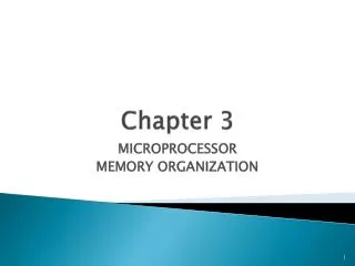
Chapter 3 MICROPROCESSOR MEMORY ORGANIZATION
Outline • 3.1 Introduction • 3.2 Main memory • 3.3 Microprocessor on-chip memory management unit and cache
3.1 Introduction • A memory unit is an integral part of any microcomputer, and its primary purpose is to hold instructions and data. • Memory system can be divided into three groups: 1. Microprocessor memory 2. Primary or main memory 3. Secondary memory
3.1 Introduction • Microprocessor memory is a set of microprocessor registers, used to hold temporary results • Main memory is the storage area in which all programs are executed, include ROM & RAM • Secondary memory (Electromechanical memory )devices such as hard disks, also called virtual memory. • The microcomputer cannot execute programs stored in the secondary memory directly, so to execute these programs the microcomputer must transfer them to its main memory by a program called the operating system.
3.2 Main memory • 8-bit microprocessors: The memory is divided into a number of 8-bit units called memory words. An 8-bit unit of data is termed a byte. Therefore, for an 8-bit microprocessor,memory word and memory byte mean the same thing.
3.2 Main memory • 16-bit microprocessors: • The memory is divided into a word contains 2 bytes (16 bits). A memory word is identified in the memory by an address. • For example, the Pentium microprocessor uses 32-bit addresses for accessing memory words. • This provides a maximum of 232 = 4,294,964,296 = 4 GB of memory addresses, ranging from 00000000,, to FFFFFFFF,, in hexadecimal.
3.2 Main memory • Intel Pentium microprocessors: • The memory is divided into segments • Segment = 216 =64KB= addressed by16bits
3.2 Main memory • Intel Pentium microprocessors (1MB): High bit for address LOW bit for segment number
3.2 Main memory • I MB memory 220 / 216 = 24 • For example, the computer uses 24 address pins to address 224= 16 MB of memory directly with addresses from 000000,, to FFFFFF,,. No. of segment =size of memory / size of one segment(216)
3.2 Main memory • An important characteristic of a memory is whether it is volatile or nonvolatile. • The contents of a volatile memory are lost if the power is turned off. • On the other hand, a nonvolatile memory retains its contents after power is switched off. ROM is a typical example of nonvolatile memory. RAM is a volatile memory.
3.2.1 Read-only Memory • ROMs can only be read, so is nonvolatile memory. • CMOS technology is used to fabricate it • ROMs are divided to: mask ROM and erasable PROM(EPROM), and EAROM (electrically alterable ROM)[also called EEPROM or E2PROM (electrically erasable PROM)]
3.2.1 Read-only Memory • Mask ROMs are programmed by a masking operation performed on a chip during the manufacturing process. The contents of mask ROMs are permanent and cannot be changed by the user. • EPROMs can be programmed, and their contents can also be altered by using special equipment, called an EPROM programmer. • When designing a microcomputer for a particular application, permanent programs are stored in ROMs. Control memories • used to microprogram the control unit are ROMs.
3.2.1 Read-only Memory • EPROMs can be reprogrammed and erased. The chip must be removed from the microcomputer system for programming. This memory is erased by exposing the chip to ultraviolet light • Typical erase times vary between 10 and 20 min.
3.2.1 Read-only Memory • EAROMs can be programmed without removing the memory from the ROM’s sockets. • These memories are also called read-mostly memories (RMMs), because they have much slower write times than read times. Therefore, these memories are usually suited for operations when mostly reading rather that writing will be performed. • Another type of memory, called Flush memory(nonvolatile), is designed using a combination of EPROM and E2PROM technologies. • Flash memory can be reprogrammed electrically while embedded on the board. An example of flash memory is used in cellular phones and digital cameras.
3.2.2 Random-Access Memory • There are two types of RAM: static RAM (SRAM), and dynamic RAM (DRAM).
3.2.2 Random-Access Memory • Two enhanced versions of DRAM are ED0 DRAM (extended data output DRAM) and SDRAM (synchronous DRAM). • The ED0 DRAM provides fast access by allowing the DRAM controller to output the next address at the same time the current data is being read. • An SDRAM contains multiple DRAMs (typically, four) internally. SDRAMs utilize the multiplexed addressing of conventional DRAMs.
3.2.3 READ and WRITE Timing Diagrams • We consider the instruction fetch, memory READ, and memory WRITE timing diagrams
3.2.3 READ and WRITE Timing Diagrams • READ timing 1. The microprocessor performs the instruction fetch cycle as before to READ the opcode. 2. The microprocessor interprets the op-code as a memory READ operation. 3. When the clock pin signal goes HIGH, the microprocessor places the contents of the memory address register on the address pins A0,-A15,, of the chip. 4. At the same time, the microprocessor raises the READ pin signal to HIGH. 5. The logic external to the microprocessor gets the contents of the location in the main ROM/RAM addressed by the memory address register and places it on the data bus. 6. Finally, the microprocessor gets this data from the data bus via pins D0, - D7, and stores it in an internal register.
3.2.3 READ and WRITE Timing Diagrams • Write timing 1. When the clock pin signal goes HIGH, the microprocessor places the contents of the memory address register on the address pins A0,-A15,, of the chip. 2. At the same time, the microprocessor raises the WRITE pin signal to HIGH. 3. The microprocessor places data to be stored from the contents of an internal register onto data pins Do-D7,. 4. The logic external to the microprocessor stores the data from the register into a RAM location addressed by the memory address register.
3.2.4 Main Memory Organization DRAM Organization • DRAMs are typically used when memory requirements are 16K words or larger. • DRAM is addressed via row and column addressing.
3.2.4 Main Memory Organization DRAM Organization • 1 -Mb (one megabit) DRAM requiring 20 address bits is addressed using 10 address lines and two control lines, RAS (row address strobe) and CAS (column address strobe). • To provide a 20-bit address into the DRAM, a LOW is applied to RAS and 1 0 bits of the address are latched. The other 10 bits of the address are applied next and CAS is then held LOW.
3.2.4 Main Memory Organization • The addressing capability of the DRAM can be increased by a factor of 4 by adding • External logic is required to generate the RAS and CAS signals and to output the current address bits to the DRAM. 220 X 4 = 220 X 22
3.2.4 Main Memory Organization • DRAM controller chips take care of the refreshing and timing requirements needed by DRAMs. DRAMs typically require a 4-ms refresh time, it sends a wait signal to the microprocessor if the microprocessor tries to access memory during a refresh cycle
3.2.5 Main Memory Array Design • Memory Array Design means: interconnecting several memory chips. • A microprocessor can address directly a maximum of 216 = 65,536 or 64K bytes of memory locations.
3.2.5 Main Memory Array Design • The control line M /IO goes LOW if the microprocessor executes an I/O instruction; it is held HIGH if the microprocessor executes a memory instruction.
3.2.5 Main Memory Array Design Chip Select M/IO
3.2.5 Main Memory Array Design Disable
3.2.5 Main Memory Array Design • To connect a microprocessor to ROM/RAM chips, two address-decoding techniques are commonly used: linear decoding and full decoding.
3.2.5 Main Memory Array Design • linear decoding Suppose we have 4K SRAM chip array comprised of the four 1K SRAM chips of Figure 3.7 See Figure 3.8
3.2.5 Main Memory Array Design • linear decoding
3.2.5 Main Memory Array Design • linear decoding Advantage does not require decoding hardware. • linear decoding Disadvantage 1. If two or more of lines A10-A13are low at the same time, more than one SRAM chip are selected, and this causes a bus conflict. Solution :software must be written such that it never reads into or writes from any address in which more than one of bits A10-A13are low.
3.2.5 Main Memory Array Design • linear decoding Disadvantage (cont.) 2. Wastes a large amount of address space. For example, whenever the address value is B800 or 3800, SRAM chip I is selected. (this situation is also called (memory foldback). Solution: To resolve problems with linear decoding, we use full decoded memory addressing. • The system of Figure 3.8 can be expanded up to a total capacity of 6K using A14, and A15, as chip selects for two more 1K SRAM chips.
3.2.5 Main Memory Array Design • full decoding. • Use Decoder In Figure 3.9 the decoder output selects one of the four IK SRAM chips, depending on the values of A12, A11, and A10(Table3.3).
3.2.5 Main Memory Array Design • Note that the decoder output will be enabled only when E3 = E2 = 0 and E l = 1. • Using 3X8 decoder, when any one of the high-order bits A15, A14,or A13, is 1, the decoder will be disabled, and thus none of the SRAM chips will be selected.
3.3 Microprocessor on-chip memory management unit and cache Typical 32-bit microprocessors such as the Pentium contain on-chip memory management unit hardware and on-chip cache memory. These topics are discussed next.
3.3.1 Memory Management Concepts • Because access to a hard disk, system throughput will be reduced to unacceptable levels. An obvious solution is to use a large and fast locally accessed semiconductor memory. Unfortunately, the storage cost per bit for this solution is very high. • A combination of both off-board disk (secondary memory) and on-board semiconductor main memory must be designed into a system.
3.3.1 Memory Management Concepts Memory management unit (MMU): a device, located between the microprocessor and memory, to control accesses,perform address mappings, and act as an interface between the logical (programmer’s memory) and physical (microprocessor’s directly addressable memory) address spaces.
3.3.1 Memory Management Concepts MMU address translation: • It translates logical program addresses to physical memory address. Note that in assembly language programming, addresses are referred to by symbolic names. • These addresses in a program are called logical addresses because they indicate the logical positions of instructions and data.
3.3.1 Memory Management Concepts MMU address translation: • The MMU can perform address translation in one of two ways: 1. By using the substitution technique [Figure 3.10(a)]. 2. By adding an offset to each logical address to obtain the corresponding physical address [Figure 3.10(b)].
3.3.1 Memory Management Concepts MMU address translation:
3.3.1 Memory Management Concepts MMU address translation: • Address translation using the substitution technique is faster than translation using the offset method. However, the offset method has the advantage of mapping a logical address to any physical address as determined by the offset value.
3.3.1 Memory Management Concepts MMU address translation: • Memory is usually divided into small manageable units: page and segment. • Paging divides the memory into equal sized pages; segmentation divides the memory into variable-sized segments. • It is relatively easier to implement the address translation table if the logical and main memory spaces are divided into pages.
3.3.1 Memory Management Concepts MMU address translation (mapping): There are three ways to map logical addresses to physical addresses: • paging, • segmentation, • and combined paging-segmentation.