Maximum Gain Amplifiers for Two-Port Network
Design and simulation of maximum gain amplifiers for a two-port network, including matching networks, patch antenna, and transistor stability.

Maximum Gain Amplifiers for Two-Port Network
E N D
Presentation Transcript
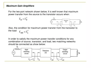
Maximum Gain Amplifiers For the two-port network shown below, It is well known that maximum power transfer from the source to the transistor occurs when: Also, the condition for maximum power transfer from the transistor to the load In order to satisfy the maximum power transfer conditions for any combination of source, transistor, and load, two matching networks should be connected as show below:
laminate Specifications Laminate consists of substrate and conductance. Substrate: dielectric constant of εr = 3.38±0.05 Thickness = t = 0.406 mm Conductance: conductivity = 5.8*106 S/m thickness of 17mm
Patch Antenna As a first step in our project we will design the passive patch antenna to operate at 15GHz frequency. From the equations the length and width of the patch are calculated to be L= 5.320 mm and W=6.757 mm.
The input impedance of antenna at 15GHz is found by plotting the real and imaginary values of Zin
The imaginary part of gamma (γ) called (β) is plotted versus frequency in order to find the exact wavelength in the circuit It was found that at 15GHz the value of (β) = 519.016 and thus λ= (2π)/ β = 12 mm.
The effect of changing the width on the performance of the antenna is simulated and the response is shown in the next figure. (1.2W (left), 1.1W, 1.0W, 0.9W, and 0.8W (right))
Transistor: It is rated to work in the 2-18GHz frequency range. The response of the S-Parameter for the transistor within the range 14 – 16 GHz are shown below
the S-parameters matrix of the transistor is different for different frequencies. At 15GHz it is specified to be as follows. The s-parameters values will be used in the schematics design simulations to represent the transistor.
Transistor stability The transistor needs to be checked for stability at the specific frequency of operation we are intending to use it at (15GHz). K = 1.0058 lΔl= 0.18819
Maximum Gain For unconditionally stable amplifier, the maximum gain can be found using the following equation. Gmax=15.21dB
Design of Matching Network The two matching networks we are designing in this section will match the transistor to the antenna and the other will match the transistor to the source. Each matching network consists of a series transmission line and a stub. We need to find the lengths of each of them for each network. reflection coefficient between transistor and the antenna reflection coefficient between transistor and the source Where Where
The equations were programmed in Matlab and produced the following values Design of Matching Network Rejected since >1 means active source accepted since <1 means passive source Rejected since >1 means active load accepted since >1 means active source
Design of Matching Network L(series)=0.472λ L(stub)=0.223λ
Design of Matching Network L(series)=0.521λ L(stub)=0.216λ
Maximum Gain Amplifier The maximum gain amplifier circuit is drawn in ADS. The design is shown in the next figure.
Maximum Gain Amplifier We can see from the curves shown above that at 15GHz the maximum gain is 15.046db and the reflection is below -40 db.
Maximum Gain AmplifierLayout A layout of the circuit with the antenna is shown in the next figure.
Design of Specified Gain Amplifier Antenna In this chapter we will design specified gain amplifiers of various specified gains (12db, 10db and 8db). The design process of specified gain amplifier circuit is similar to that of the maximum gain amplifier design. The difference however lies in the matching networks only. laminate Specifications The same substrate that was used for the maximum gain amplifier antenna is used for the design of the specified gain active antenna. The substrate has a dielectric constant of er = 3.38±0.05. The substrate is 0.406 mm thick and the metal used is copper with specified conductivity of 5.8*106 S/m and a thickness of 17mm. Patch Antenna The patch antenna that was designed in the previous chapter is used for the design of the specified gain active antenna. The impedance of the antenna at 15GHz was found to be Zin = 51.709+j2.267 ohm.
Design of Specified Gain Amplifier Antenna Transistor: The same transistor that was used in the maximum design antenna is used for the design of the specified gain active antenna. The s-parameters values will be used in the schematics design simulations to represent the transistor. The transistor was determined to be unconditionally stable at 15 GHz.
Design of Specified Gain Amplifier Antenna in some cases, it is required to design the amplifier for a specific value of the gain rather than the maximum value. This specific value of the gain can be achieved by designing the input and output matching circuits to provide values for and different from those required for maximum gain and To simplify the analysis, a unilateral transistor is considered. For most practical cases transistor is very small, such that it behaves effectively as unilateral, The error caused by unilateral approximation is given by: where: U = unilateral figure of merit The expression of the unilateral transducer gain, which has been proved before, can be decomposed into three gain factors as follows:
Design of Specified Gain Amplifier Antenna The expression of the unilateral transducer gain, which has been proved before, can be decomposed into three gain factors as follows: where: , , source gain factor load gain factor constant gain factor
Design of Specified Gain Amplifier Antenna Similar decomposition can be performed for the expression of the maximum unilateral transducer gain: where: maximum source gain maximum load gain
Design of Specified Gain Amplifier Antenna Now, the normalized gain factors can be defined as follows: normalized source gain factor = where normalized load gain factor where
Design of Specified Gain Amplifier Antenna Matching Network After the derivation of equations 26 and 27 we get equation of the constant circle in the plane), where: center of the constant circle radius of the constant circle
Design of Specified Gain Amplifier Antenna Matching Network Similar treatment of equation (27), yields the equation of the constant gL circle in the ΓL plane: (equation of the constant circle in the plane), where c center of the circle constant radius of the circle
Design of Specified Gain Amplifier Antenna Matching Network We then developed a Matlab program to the values of the error and Cs , Rs , CL , and RL for the source and load respectively. The error was found to be the following. Using the Matlab program we found the values of Cs , Rs , CL , and RL and marked them on smith chart to find the values ofFor the gains 12, 10 and 8 db and
Design of Specified Gain Amplifier Antenna Matching Network Gain of 12db 0.55~-147’ 0.18143 L(series)=0.05λ L(stub)=0.103λ
Design of Specified Gain Amplifier Antenna Matching Network Gain of 12db 0.3089~171’ 0.23965 L(series)=0.146λ L(stub)=0.024λ
Design of Specified Gain Amplifier Antenna The 12db specified gain amplifier circuit is drawn in ADS. The design is shown in the next figure.
Design of Specified Gain Amplifier Antenna The simulation of the circuit shown above produces the following response that is shown in the following figure. We can see from the curves shown above that at 15GHz the maximum gain is 11.926db and the reflection is below -10.955 db
Design of Specified Gain Amplifier Antenna A layout of the circuit with the antenna is shown in the next figure.
Design of Specified Gain Amplifier Antenna Matching Network Gain of 10db 0.4693~-147’ 0.3727 L(series)=0.07λ L(stub)=0.027λ
Design of Specified Gain Amplifier Antenna Matching Network Gain of 10db 0.25062~171’ 0.46974 L(series)=0.382λ L(stub)=0.065λ
Design of Specified Gain Amplifier Antenna The 10db specified gain amplifier circuit is drawn in ADS. The design is shown in the next figure.
Design of Specified Gain Amplifier Antenna The simulation of the circuit shown above produces the following response that is shown in the following figure We can see from the curves shown above that at 15GHz the maximum gain is 10.057db and the reflection is below -5.705 db.
Design of Specified Gain Amplifier Antenna A layout of the circuit with the antenna is shown in the next figure.
Design of Specified Gain Amplifier Antenna Matching Network Gain of 8db 0.3948~-147’ 0.49605 L(series)=0.325λ L(stub)=0.032λ
Design of Specified Gain Amplifier Antenna Matching Network Gain of 8db 0.2025~171’ 0.60041 L(series)=0.356λ L(stub)=0.11λ
Design of Specified Gain Amplifier Antenna The 8db specified gain amplifier circuit is drawn in ADS. The design is shown in the next figure.
Design of Specified Gain Amplifier Antenna The simulation of the circuit shown above produces the following response that is shown in the following figure We can see from the curves shown above that at 15GHz the maximum gain is 8.167db and the reflection is below -3.831 db.
Design of Specified Gain Amplifier Antenna A layout of the circuit with the antenna is shown in the next figure.
Wilkinson Power divider It has been demonstrated before that one way of increasing the bandwidth of the amplifier is to design for less than the maximum gain. However, the return loss of the reduced gain amplifier becomes relatively large even at the design frequency. To overcomes the return loss problem, while maintaining the gain flatness, a power divider circuit such as that shown below is used: RS ZL
Wilkinson Power divider There have three type of power divider. Wilkinson Power divider Lossless T-Junction Resistive T-Junction
Wilkinson Power divider λ /4 λ /4