Download
1 / 33
330 likes | 434 Vues
Learn about SPICE functions, component libraries, analysis types, source files, conventions, and more. Utilize SPICE for circuit design and analysis.

E N D
Introduction to SPICE • SPICE was originally developed at the University of California, Berkeley (1975). • Simulation Program for Integrated Circuits Emphasis • HSPICE = High-performance SPICE • PSpice = PC version of SPICE
SPICE Functions • DC analysis: DC transfer curve • Transient analysis: voltage and current as a function of time • AC Analysis: output as a function of frequency • Noise analysis • and more …. • SPICE has analog and digital libraries for standard components (Transistor, NAND, NOR, …) • Different temperatures • Default temperature is 300K
Components • Independent voltage and current sources • Dependent voltage and current sources • Resistor • Capacitor • Inductor • Operational amplifier • Transistor • Digital gates …
SPICE Source File • Title statement: first line • Data statements: specify the Circuit, components,interconnections • Control statements: specify what types of analysis to perform on the circuit. • Output statements: specify outputs • Comment statements: begin with an asterisk (*) • End statement: .END <carriage return> • "+" sign (continuation sign)
Suffixes • T Tera (10+12) • G Giga (10+9) • MEG Mega (10+6) • K Kilo (10+3) • M Mili (10-3) • U Micro (10-6) • N Nano (10-9) • P Pico (10-12) • F Femto (10-15)
N1(+) N1(+) N2(-) N2(-) Independent DC Sources • Voltage source: Vname N+ N- Type Value • Current source: Iname N+ N- Type Value • Type: DC, AC or TRAN (transient) (like PULSE, …) • Vin 2 0 DC 10 • Vin 2 0 AC 10 • Is 3 4 DC 1.5 • Voltage and Current Conventions
Dependent DC Sources • Voltage controlled voltage source: • Ename N+ N- NC+ NC- Value • Voltage controlled current source: • Gname N+ N- NC+ NC- Value • Current controlled voltage source: • Hname N+ N- Vmeas Value • Current controlled current source: • Fname N+ N- Vmeas Value • N+ and N- are terminals of the dependent source • NC+ and NC- are terminals of the controlling voltage source
N- Vmeas Vmeas N+ Ename N+ N- NC+ NC- α Gname N+ N- NC+ NC- γ Hname N+ N- Vmeas ρ Fname N+ N- Vmeas β
Example F1 0 3 Vmeas 0.5 Vmeas 4 0 DC 0
3 + 5V 1pF _ 4 Resistors, Capacitors, Inductors • Rname N+ N- Value • Cname N+ N- Value <IC> • Lname N+ N- Value <IC> • IC = initial condition (DC voltage or current) Example: C1 3 4 1pF 5V C2 1 2 2pF L1 3 4 1mH L2 7 3 2mH 1mA
Damped Sinusoidal Sources • Vname N+ N- SIN(VO VA FREQ TD THETA PHASE) • VO - offset voltage in volt. • VA - amplitude in volt. • f = FREQ in Hz • TD - delay in seconds • THETA - damping factor per second • Phase - phase in degrees • If TD, THETA and PHASE are not specified, it is assumed to be zero. Example: V1 1 2 SIN(5 10 50 0.2 0.1) V2 3 4 SIN(0 10 50)
Piecewise linear source (PWL) • Vname N+ N- PWL(T1 V1 T2 V2 T3 V3 ...) • Vi is the value source at time Ti • Example: Vg 1 2 PWL(0 0 10U 5 100U 5 110U 0)
Pulse • Vname N+ N- PULSE(V1 V2 TD TrTf PW Period) • V1 - initial voltage • V2 - peak voltage • TD - initial delay time • Tr - rise time • Tf - fall time • pw- pulse-width • Period - period
Subcircuits • A subcircuit allows you to define a collection of elements as a subcircuit (e.g. an operational amplifier) .SUBCKT SUBNAME N1 N2 N3 ... Element statements . .ENDS SUBNAME • N1, N2, N3 are the external nodes of the subcircuit. The external nodes cannot be 0. • The node numbers used inside a subcircuit are strictly local, except for node 0 which is always global.
Example: µ741 (Op Amp) * Subcircuit for 741 op amp * +in (=1) -in (=2) out (=3) .subckt opamp741 1 2 3 rin 1 2 2meg rout 6 3 75 e1 4 0 1 2 100k r1 4 5 0.5meg c1 5 0 31.85nf eout 6 0 5 0 1 .ends opamp741
Using Subcircuit vs 1 0 dc 5 r1 1 2 200 rf 2 3 1k x1 0 2 3 opamp741 .dc vs 0 10 1 .option post .end
.OP Statement • Instructs SPICE to compute DC operating points • voltage at each node • current in each voltage source • operating point for each element
.DC Statement • Increment (sweep) an independent source over a certain range with a specified step .DC SRCname START STOP STEP • SRCname = name of the source • START and STOP = starting and ending values • STEP = size of increments • Example: .DC V1 0 20 2
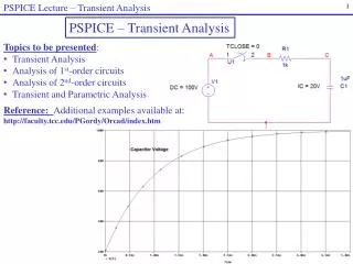
.TRAN Statement • Specifies time interval for transient analysis .TRAN TSTEP TSTOP <TSTART> • TSTEP = increment • TSTOP = final time • TSTART = starting time
.AC Statement • Specify frequency (AC) analysis .AC LIN NP FSTART FSTOP • LIN = linear frequency variation • NP = number of points. • FSTART and FSTOP = start and stopping frequencies (Hz) • Example: .AC LIN 10 1000 2000
Output Statements • .PLOT plots selected output variables, to design.lis using ASCII characters. .PLOT is useful for looking at plotted results without access to AvanWaves. • .PRINT DC V(2) prints node voltage value for node 2 in the design.lis file.
.PRINT & .PLOT • .PRINT TYPE OV1 OV2 OV3 ... • .PLOT TYPE OV1 OV2 OV3 ... • TYPE = type of analysis printed or plotted • DC • TRAN • AC • OV1, OV2 = output variables Examples: .PLOT DC V(1,2) V(3) I(Vmeas) .PRINT TRAN V(3,1) I(Vmeas)
* We are interested in finding the following characteristics: * 1. Node voltages v12, v2 and current i4 when vin=10V * 2. Thevenin equivalent voltage and resistance, seen * at the output terminals v(3,0) VIN 1 0 DC 10 VMEAS 4 0 DC 0 *VMEAS is a 0V source to measure i4 F1 0 3 VMEAS 0.5 R1 1 2 1K R2 2 3 10K R3 1 3 15K R4 2 4 40K R5 3 0 50K .tran .01n 50n .TF V(3,0) VIN .DC VIN 0 20 2 .PLOT DC V(1,2) .END
* pulse generator * +node -node V1 V2 TD TR TF PW PER VIN 1 0 PULSE ( 0 5 0 0.1N 0.1N 50N 100N) R1 1 2 10M R2 2 0 10M C1 2 0 1uF * transient simulation for 50ns with 0.01ns step size .tran .1n 500n * dc simulation with stimulus voltage (source VIN) from 0 to 5V in 0.1V steps .DC VIN 0 5 0.01 .end
5 2 1 - 5V46 10 10 + 10V _ + 3 5 6 5 10 10 10 0 4 5 Example 3 * TheveninVs 1 0 DC 10VE1 3 2 4 6 5R1 1 2 5R2 1 4 5R3 0 4 5R4 3 4 10R5 2 5 10R6 2 6 10R7 5 4 10R8 4 6 10.TF V(5,6) Vs.plot DC V(5,6).plot DC I(Vs).DC Vs 0 100 10.END
OLD_HW1_Solution * Thevenin Vs 2 5 DC 100V Vmeas 2 3 DC 0V Fx 6 7 Vmeas 4.0 Ex 2 1 5 4 3.0 R1 3 4 5.0 R2 4 7 5.0 R3 5 4 4.0 R4 7 0 4.8 R5 5 6 1.0 R10 1 0 1MEG .TF V(4,0) Vs .plot DC V(5,4) .plot DC V(1,0) .plot DC I(Vmeas) .DC Vs 0 100 10 .tran 1n 50n 0 .END
Example 5 1 2 0
OLD_HW2_Solution Vs 1 0 AC 1 L1 1 2 1m C1 1 2 1n R1 2 0 10M .AC LIN 10 1000 2000 plot AC V(1,2) I(Vs) .END