Download
1 / 7
70 likes | 129 Vues
Learn why materials like copper, silicon, and quartz exhibit high, variable, or low conductivity when atoms form solids. Explore allowed, empty, and occupied electronic energy levels and bands in materials. Discover how silicon and doped silicon conduct electricity at different temperatures.

E N D
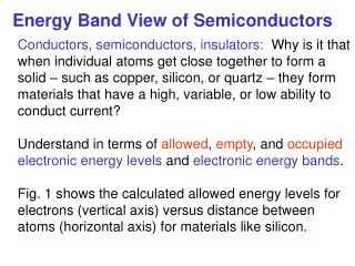
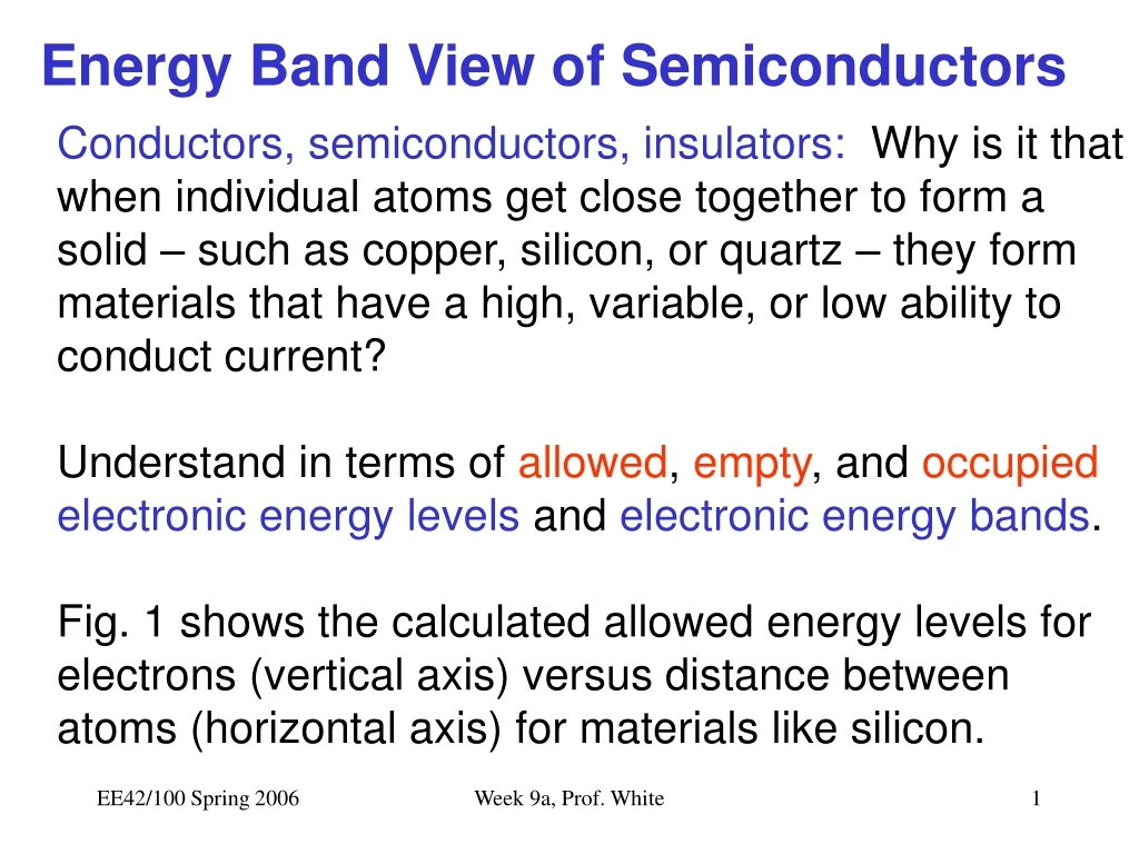
Energy Band View of Semiconductors Conductors, semiconductors, insulators: Why is it that when individual atoms get close together to form a solid – such as copper, silicon, or quartz – they form materials that have a high, variable, or low ability to conduct current? Understand in terms of allowed, empty, and occupiedelectronic energy levels and electronicenergy bands. Fig. 1 shows the calculated allowed energy levels for electrons (vertical axis) versus distance between atoms (horizontal axis) for materials like silicon. Week 9a, Prof. White
Fig. 1. Calculated energy levels in the diamond structure as a function of assumed atomic spacing at T = 0o K. (From “Introduction to Semiconductor Physics”, Wiley, 1964) Week 9a, Prof. White
In Fig. 1, at right atoms are essentially isolated; at left atomic separations are just a few tenths of a nanometer, characteristic of atoms in a silicon crystal. • If we start with N atoms of silicon at the right, which have 14 electrons each, there must be 14N allowed energy levels for the electrons. (You learned about this in physics in connection with the Bohr atom, the Pauli Exclusion principle, etc.) • If the atoms are pushed together to form a solid chunk of silicon, the electrons of neighboring atoms will interact and the allowed energy levels will broaden intoenergy bands. Week 9a, Prof. White
When the “actual spacing” is reached, the quantum-mechanical calculation results are that: • at lowest energies very narrow ranges of energy are allowed for inner electrons (these are core electrons, near the nuclei); • a higher band of 4N allowed states exists that, at 0oK, is filled with 4N electrons; • then an energy gap, EG, appears with no allowed states (no electrons permitted!); and • at highest energies a band of allowed states appears that is entirely empty at 0oK. • Can this crystal conduct electricity? Week 9a, Prof. White
NO, it cannot conductor electricity at 0o K because that involves moving charges and therefore an increase of electron energy – but we have only two bands of states separated by a forbidden energy gap, EG. The (lower) valence band is entirely filled, and the (upper) conduction band states are entirely empty. To conduct electricity we need to have a band that has some filled states (some electrons!) and some empty states that can be occupied by electrons whose energies increase. Week 9a, Prof. White
Metals, pure silicon at 0K and 300K, and doped silicon • A. Conductors such as aluminum and gold can conduct at low • temperatures because the highest energy band is only partly • filled – there are electrons and there are empty states they can • move into when caused to move by an applied electric field. • B. Silicon at 0K – can’t conduct because the highest band containing • electrons is filled. • Pure silicon at room temp. is slightly conductive since thermal • energy can raise some electrons to the mostly empty conduction • band. • Silicon doped with donors (like P or As) can conduct (and become • n-type) better than pure silicon at room temp. since it doesn’t take • much energy to free a valence electron so it can enter the conduction • band. • Silicon doped with acceptors (like B) can conduct (and become • p-type) at room temp. since it doesn’t take much energy to free a • valence electron and create a hole in the valence band. Week 9a, Prof. White
A. Metal B. Pure Si 0K C. Pure Si at 300K D. n-type Si E. p-type Si Conduction band + + + Forbidden energy band (energy gap) Donor level Acceptor level - - - Valence band Week 9a, Prof. White