Download
1 / 2
20 likes | 163 Vues
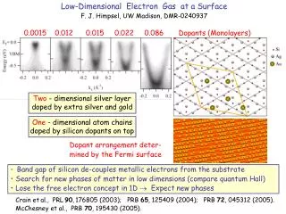
Low-Dimensional Electron Gas at a Surface F. J. Himpsel, UW Madison, DMR-0240937. 0.0015 0.012 0.015 0.022 0.086 Dopants (Monolayers). Two - dimensional silver layer doped by extra silver and gold. One - dimensional atom chains doped by silicon dopants on top.

E N D
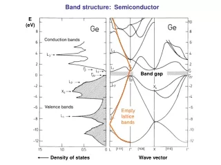
Low-Dimensional Electron Gas at a Surface F. J. Himpsel, UW Madison, DMR-0240937 0.0015 0.012 0.015 0.022 0.086 Dopants (Monolayers) Two - dimensional silver layer doped by extra silver and gold One - dimensional atom chains doped by silicon dopants on top Dopant arrangement deter- mined by the Fermi surface • Band gap of silicon de-couples metallic electrons from the substrate • Search for new phases of matter in low dimensions (compare quantum Hall) • Lose the free electron concept in 1D Expect new phases Crain etal., PRL90,176805 (2003); PRB 65, 125409 (2004); PRB 72, 045312 (2005). McChesney et al., PRB 70, 195430 (2005).
Educate Students and the Public on Nanoscience and Nanotechnology Make International Connections • The PI received a Humboldt Award in 2005 to work on atomic chains in Germany. • While in Germany he gave tutorial lectures on nanoscience and nanotechnology to • international students receiving a DAAD fellowship (Berlin, July 2, 2005) and to • graduate students at the University Erlangen (July 6 and 13, 2005). • The PI was lead-off speaker at Nano-Expo, Madison, May 30-31, 2003 and appeared on a • video about nanotechnology produced for the general public on this occasion. He gave a • half-hour interview about nanotechnology at the WORT radio station (April 17, 2005). • The PI taught a popular graduate course on nanoscience and technology (38 students). • The PI co-organized a NSF/EC Workshop on Nanotechnology, Grenoble, June 12-14, 2002. • DMR-0211829; ftp://ftp.cordis.lu/pub/nanotechnology/docs/nano_grenoble_proceedings_en_1102.pdf • Jason Crain graduated in 2003 after receiving the 2002 Aladdin Lamp Award of the • Synchrotron Radiation Center (SRC) for his work on one-dimensional electrons. • He received a NRC postdoctoral fellowship at NIST and is now staff member at NIST. • Jessica McChesney graduated in 2004 after receiving the 2003 Aladdin Lamp Award • of the SRC and is now postdoc working at the Advanced Light Source in Berkeley. • She presented her results to Representative Vernon Ehlers on a visit to Madison. • Her image of an atomic scale memory was selected for the American Vacuum Society's • nanotechnology poster: http://divisions.avs.org/nstd/PosterNSTD.pdf